

Semiconductor device and method for fabricating the same
a technology of semiconductors and semiconductors, applied in mechanical devices, transportation and packaging, gearing, etc., can solve the problems of limiting the performance improvement of polysilicon tft, difficult to integrate controllers, da converters and other functional circuits, and difficult in practice to achieve the effect of reducing the level differen
- Summary
- Abstract
- Description
- Claims
- Application Information
AI Technical Summary
Benefits of technology
Problems solved by technology
Method used
Image

Examples
embodiment 1
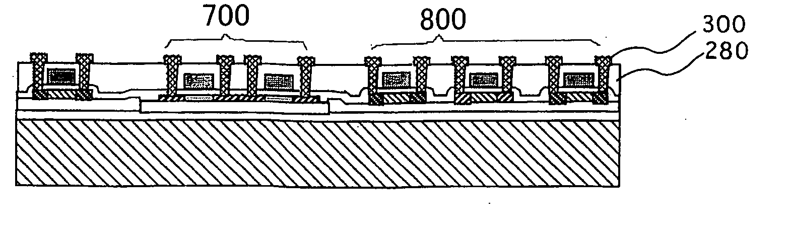
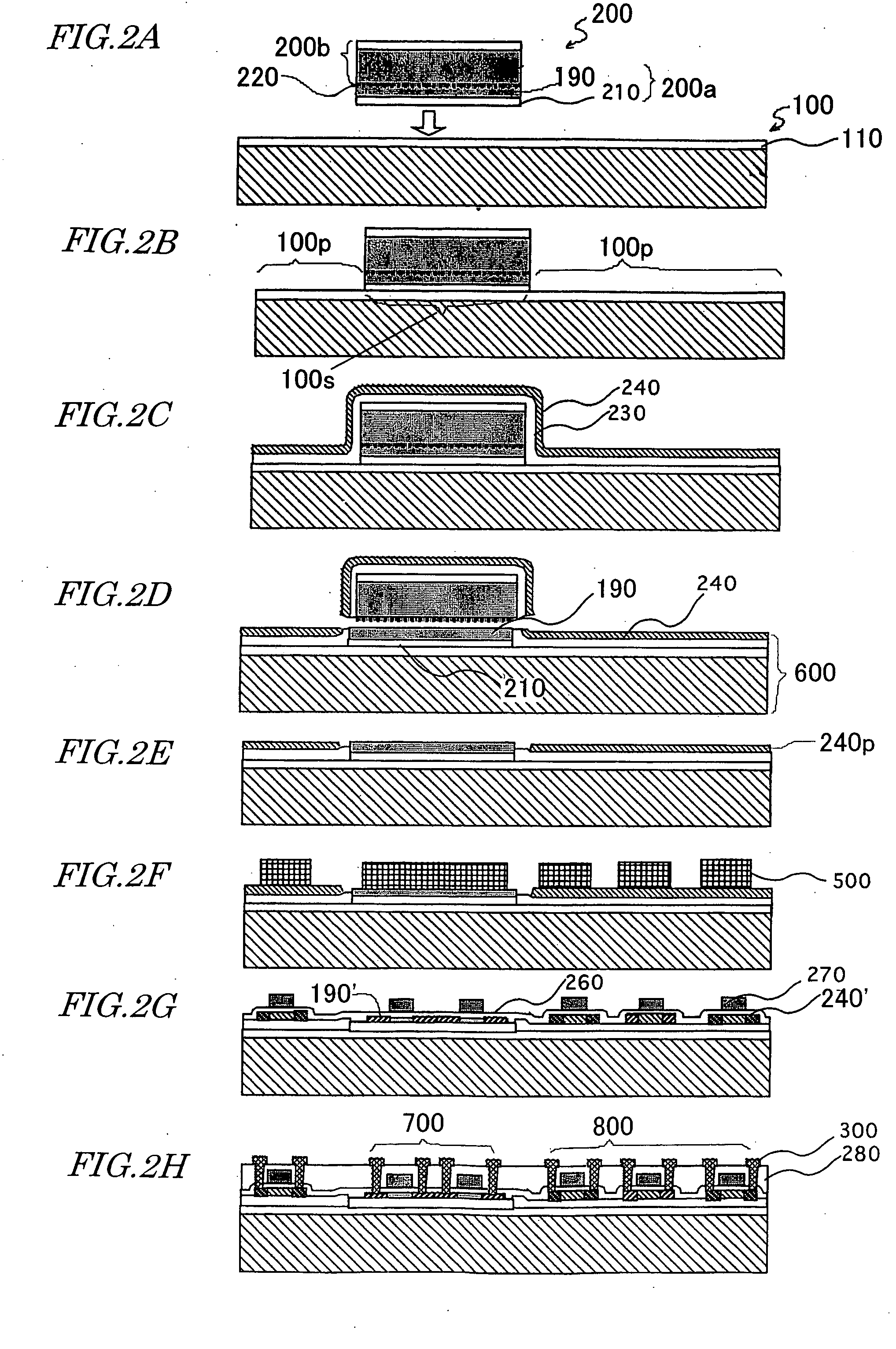
[0073] Hereinafter, a first specific preferred embodiment of the present invention will be described with reference to FIGS. 2A through 2H.
[0074] First, as shown in FIG. 2A, a supporting substrate 100 and a single crystal silicon substrate 200 are prepared. Although only one single crystal silicon substrate 200 is illustrated in FIG. 2A, the number of single crystal silicon substrates 200 to be bonded onto the single supporting substrate 100 does not have to be one but may be two or more.
[0075] In this preferred embodiment, the supporting substrate 100 is a glass substrate Code 1737 (produced by Corning Inc.) on which an SiO2 film 110 has been deposited to a thickness of about 100 nm. This SiO2 film 110 may be deposited by a plasma CVD process using tetraethylorthosilicate (TEOS) and oxygen gases. The SiO2 film 110 may be omitted depending on the material of the substrate. For example, when the glass substrate Code 1737 is used, it is not always necessary to deposit an insulating ...
embodiment 2
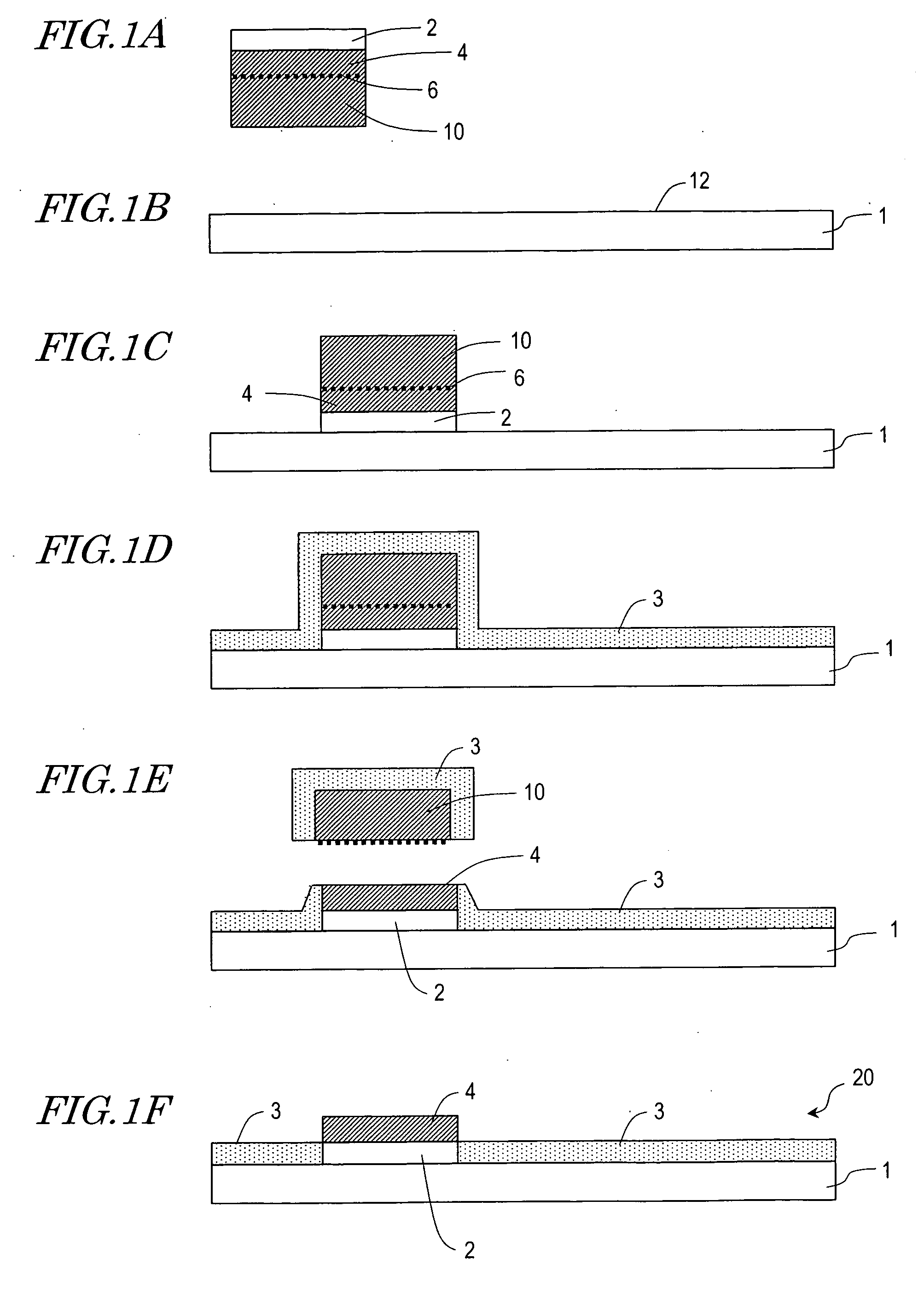
[0098] Hereinafter, a second specific preferred embodiment of the present invention will be described with reference to FIGS. 3A through 3I.
[0099] First, as shown in FIG. 3A, a supporting substrate 100 and a single crystal silicon substrate 200 are prepared. Each of the supporting substrate 100 and single crystal silicon substrate 200 may have the same configuration as, and may be prepared by the same method as, the counterpart that has already been described for the first preferred embodiment with reference to FIG. 2A. In FIG. 3A, the first SiO2 film 210 of the single crystal silicon substrate 200 is illustrated as if the film 210 were thinner than the first SiO2 film 210 shown in FIG. 2A. Actually, however, these two films have approximately equal thicknesses. In this manner, the thicknesses and sizes of respective layers are not always to scale in not only FIG. 3A but also the other drawings as well. Thus, the present invention is in no way limited to the configurations illustra...
embodiment 3
[0117] Hereinafter, a third specific preferred embodiment of the present invention will be described with reference to FIGS. 4A through 4H.
[0118] In the bonded substrate 602 of this preferred embodiment, a transistor structure including a single crystal silicon layer is defined on the first insulating layer 210 as shown in FIG. 4D unlike the bonded substrate 600 shown in FIG. 2D.
[0119] First, as shown in FIG. 4A, a supporting substrate 100 and a single crystal silicon substrate 201 are prepared. The supporting substrate 100 may have the same configuration as, and may be prepared by the same method as, the counterpart described for the first preferred embodiment with reference to FIG. 2A.
[0120] On the other hand, the single crystal silicon substrate 201 may be prepared in the following manner.
[0121] First, a first SiO2 film 210 is deposited to a thickness of 50 nm to 100 nm, for example, on the surface of a single crystal silicon wafer. In this preferred embodiment, the first SiO...
PUM
 Abstract
Description
Claims
Application Information