Thin film transistor array inspection device

a transistor array and inspection device technology, applied in semiconductor/solid-state device testing/measurement, fault location by increasing destruction at fault, instruments, etc., can solve the problems of difficult to detect defects with high precision, difficult to discriminate between normal pixel and defective pixel, etc., to achieve constant precision

Inactive Publication Date: 2005-08-11
SHIMADZU CORP
View PDF5 Cites 19 Cited by
  • Summary
  • Abstract
  • Description
  • Claims
  • Application Information

AI Technical Summary

Benefits of technology

[0028] According to the present invention, even when the size of the pixel electrode of the TFT is changed, it is possible to detect a defect with constant precision without an influence of the change.

Problems solved by technology

As a result, it is difficult to discriminate between the normal pixel and the defective pixel.
Accordingly, it is even more difficult than the case in FIG. 12(b) to discriminate between a normal pixel and a defective pixel.
Accordingly, it is difficult to detect a defect with high precision due to the relationship between the irradiation area of the charged particle beam and the pixel electrode as mentioned above.
Further, when a shape of the pixel electrodes is changed, it is difficult to detect a defect with constant precision due to a difference in shapes between the irradiation area of the charged particle beam and the pixel electrode.

Method used


Image

  • Thin film transistor array inspection device
  • Thin film transistor array inspection device
  • Thin film transistor array inspection device

Examples


Embodiment Construction

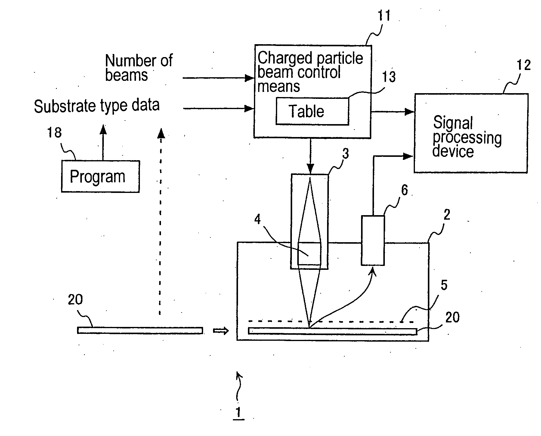
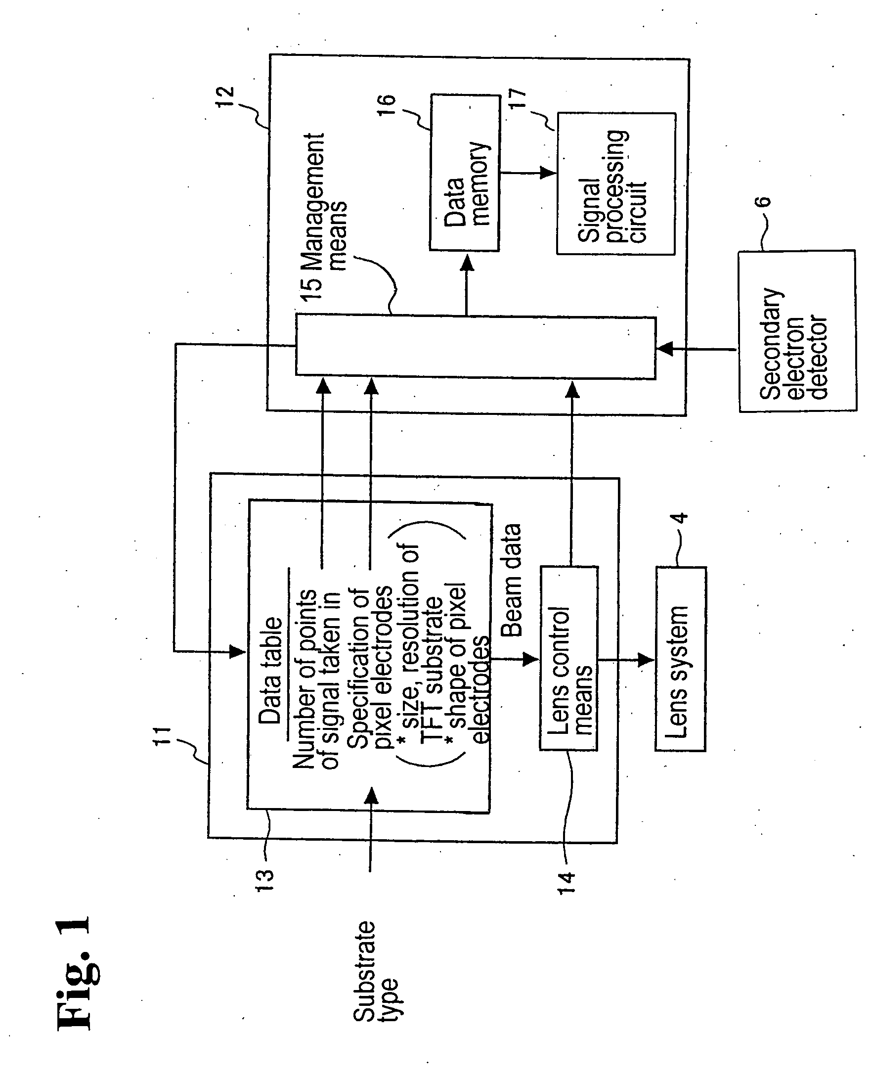
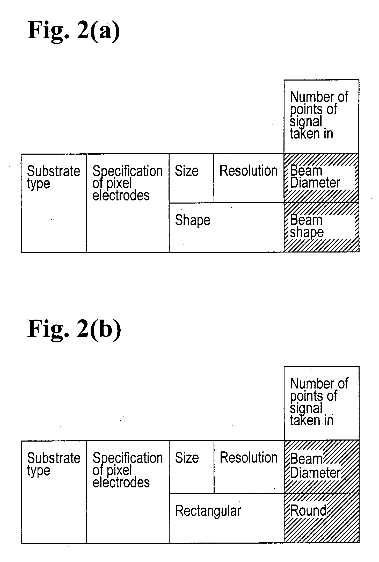
[0041] Hereunder, embodiments of the present invention will be explained with reference to the accompanying drawings. FIG. 1 is a block diagram for explaining a general configuration of a TFT array inspection device according to an embodiment of the present invention. In FIG. 1, a TFT substrate as an object of inspection, a charged particle beam source for irradiating a charged particle beam on the TFT substrate, a device for scanning the charged particle beam, and a chamber are omitted.

[0042] In FIG. 1, the charged particle beam source (not shown) generates the charged particle beam. The charged particle beam is formed in a specific beam shape with a specific beam size by an electrostatic lens (magnetic lens) 4, and is radiated on the TFT substrate (not shown). Secondary electrons are emitted from the TFT substrate irradiated with the charged particle beam, and are detected by a secondary electron detector 6. A signal processing device 12 processes a secondary electron signal dete...


PUM

PropertyMeasurementUnit
sizeaaaaaaaaaa
sizeaaaaaaaaaa
sizeaaaaaaaaaa

Abstract

A TFT array inspection device inspects a TFT array by irradiating a TFT substrate with a charged particle beam and detecting secondary electrons produced from a pixel electrode of the TFT substrate by irradiation of the charged particle beam. The TFT array inspection device includes a charged particle beam control device for changing at least one of a size and a shape of the charged particle beam in accordance with at least one of a specification of the pixel electrode and a number of detection points on the pixel electrode.

Description

BACKGROUND OF THE INVENTION AND RELATED ART STATEMENT [0001] The present invention relates to a TFT array inspection device, and in particular, to an inspection device for inspecting a defective pixel and performance of a thin film transistor array (TFT array) used for a liquid crystal display, an organic EL display, and the like, using a charged particle beam and measurement data. [0002] As a configuration in which TFTs (thin film transistors) are arranged in an array form, for example, there is a liquid crystal substrate used for a flat panel display (FPD) of a liquid crystal display and the like. A liquid crystal display formed of the TFTs has a basic structure of a liquid crystal panel in which a liquid crystal is filled in a space between one glass substrate on which the TFTs and pixel electrodes are formed and another glass substrate on which opposing electrodes are formed. [0003] The glass substrate has a plurality of panels formed with a common fabrication process of integra...

Claims


Application Information

Patent Timeline
Patent Type & Authority Applications(United States)
IPC IPC(8): G01R31/00G02F1/1368G01R31/305H01L21/66H01L29/786H01L51/50H05B33/14
CPCG01R31/305
Inventor IWASAKI, KOTA
Owner SHIMADZU CORP
Why Eureka
Try Eureka