Depositing solid materials

Inactive Publication Date: 2005-08-11
QINETIQ LTD
View PDF15 Cites 87 Cited by
  • Summary
  • Abstract
  • Description
  • Claims
  • Application Information

AI Technical Summary

Benefits of technology

[0013] In an alternative aspect of the invention, the fluids react to yield a chemically active species. This can,

Problems solved by technology

In the case of inkjet printing however, many solids present difficulties in be

Method used


Image

  • Depositing solid materials
  • Depositing solid materials

Examples


first embodiment

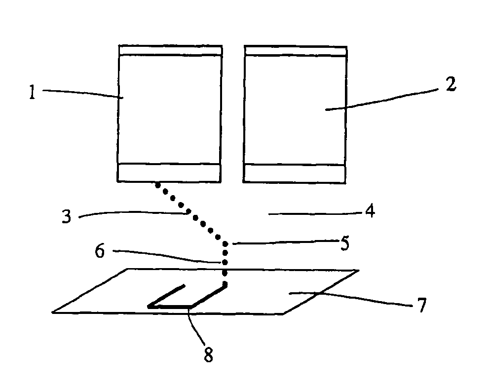
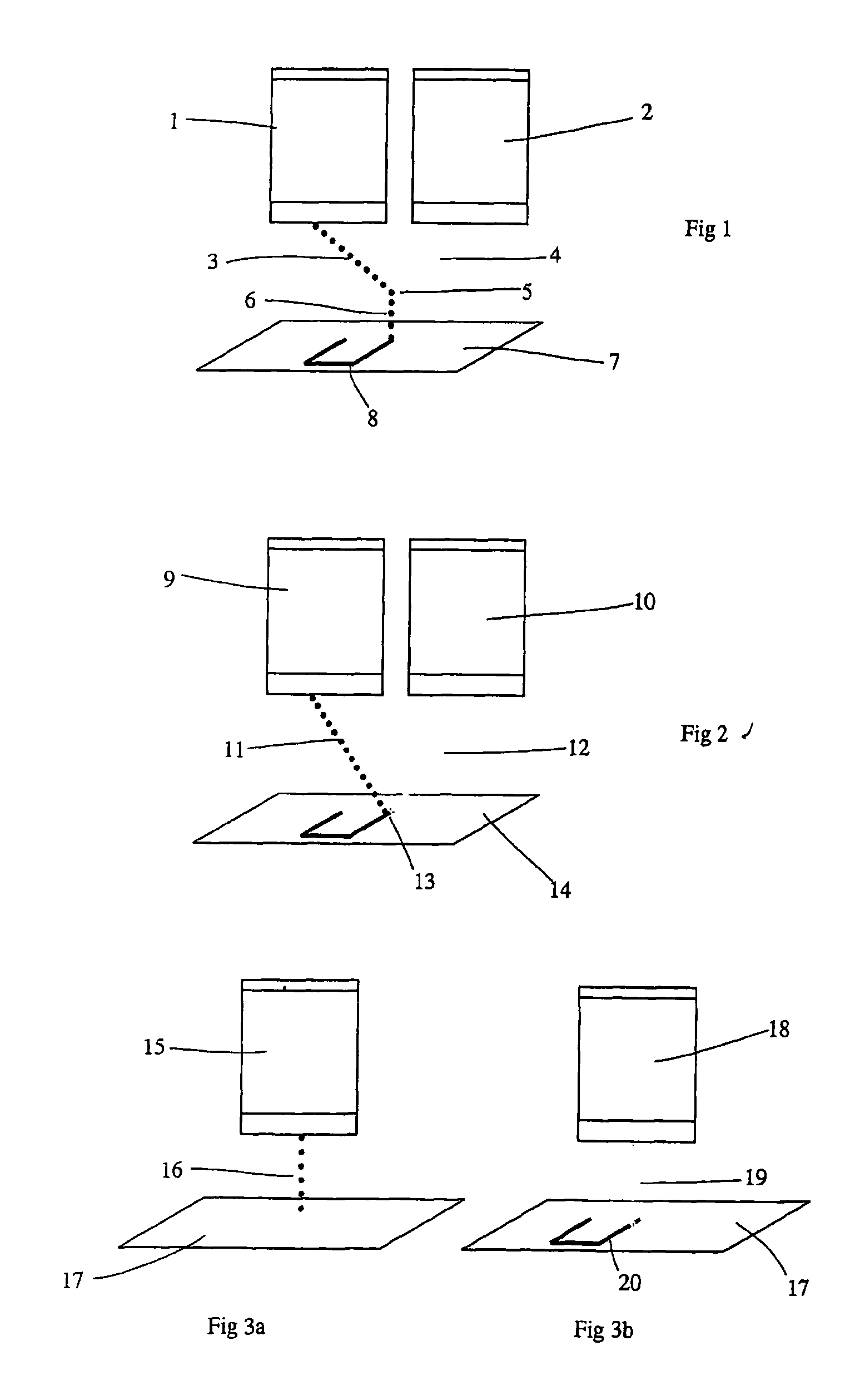
[0018] In a first embodiment, the inkjet printer prints a PCB conductor by simply printing the metal salt and the reducing agent directly, instead of red and green ink (for example). The advantage is therefore in removing the need for the usual electroless bath process and its associated stabilisers. The PCB can be printed to the resolution of the inkjet printer, typically 20 μm at present as noted above.

second embodiment

[0019] In a second embodiment, reactive inks containing solvated species are combined to produce ceramic materials which may be in their final or alternatively “green” states. The “green” state refers to an intermediate ceramic material that has then to be sintered into its final form. Examples include hydroxides, carbonates or oxides of metals. The advantage of this approach is that reactions at the substrate result in improved material conformity with the substrate and the formation of a more dense material after this and subsequent processes, as compared to for example the printing of inks having the same solids contained in an organic binder. The ceramic layer can thus be built into two or three-dimensional structures. The resulting ceramic may have a wide range of properties, for example it may be an insulator such as calcium carbonate or a transparent conductor, such as zinc oxide. To print a three-dimensional article, a pair of fluids can be used which react to give a precipi...

third embodiment

[0020] In a third embodiment, sequential inkjet printing of a variety of materials is proposed, to build up multiple layers with differing properties. For example, inks could react together to form solid deposits of dielectrics such as ceramics or conductors hereinbefore described, or alternatively adhesive-like layers such as epoxy resins from two part inks. These types of materials may then be deposited sequentially in a user-defined way from an array of inkjet heads. The layers may also be combined with those formed more simply using dried inks from single inkjet heads. Thus, two processes could be combined for example to produce electrical components. In this way a conductive area could be formed, followed by a thin dielectric layer and further covered with conductor to form a capacitor as part of a PCB layout.

[0021] A further advantage of the present invention is that the process line may employ a larger series of inkjet heads beneath which substrates undergo a single pass at g...


PUM

PropertyMeasurementUnit
Fractionaaaaaaaaaa
Dielectric polarization enthalpyaaaaaaaaaa
Solubility (mass)aaaaaaaaaa

Abstract

Material can be deposited directly onto a substrate by using a fluid applicator such as an inkjet printer to apply at least two fluids which react to give the desired material for a range of applications. Thus, multiples of a printing mechanism are used to deposit materials as reagents that react together to form products. The materials may also be advantageously deposited from multiple inkjet heads to prepare a wide range of reaction scenarios in the form of user-defined patterns which may be sequences of differing layers and possibly to build up thicker layers. Thus, a PCB could be printed by the inkjet printer by simply printing the metal salt and the reducing agent directly, instead of two colours from a conventional inkjet printer for example. To print a three dimensional article, a pair of fluids which react to give a precipate can be used instead. Repeated passes can then build up a desired shape. The two processes could be combined to produce composite devices such as electrical components.

Description

FIELD OF THE INVENTION [0001] The present invention relates to the deposition of solid materials. It provides a method of doing so, and a printer for doing so. BACKGROUND ART [0002] The production of printed circuit boards (PCBs) is a major market that has expanded with the rise in electronic, computing and other such industries. As the process of electronic integration has developed, there has been a corresponding demand for finer and more accurate detail in the PCB production process, with narrower conductive tracks and greater densities of components. Finer tracks ease the use of surface mount technologies such as ‘flip chip’ or the like. Electroless deposition is used to coat whole surfaces, and the formation of metal patterns requires additional and costly processing such as photolithography and etching. Existing PCB technology uses lithographic techniques to obtain a resolution of 50 μm, but this is an optimal outcome that is not typically available over the whole of a large P...

Claims


Application Information

Patent Timeline
IPC IPC(8): B05C5/00B05C9/06B05D1/26B41J2/01B41M3/00C23C18/16H05K3/10H05K3/12H05K3/18
CPCB05C9/06B41J2/01B41M3/001B41M3/008H05K3/125C23C18/1655C23C18/161C23C18/16C23C18/1608C23C18/31H05K3/182B33Y30/00B41J2/17
Inventor JOHNSON, DANIEL RDAMERELL, WILLIAM N.KYNASTON-PEARSON, ANTHONY W.N.
Owner QINETIQ LTD
Why Eureka
Try Eureka