

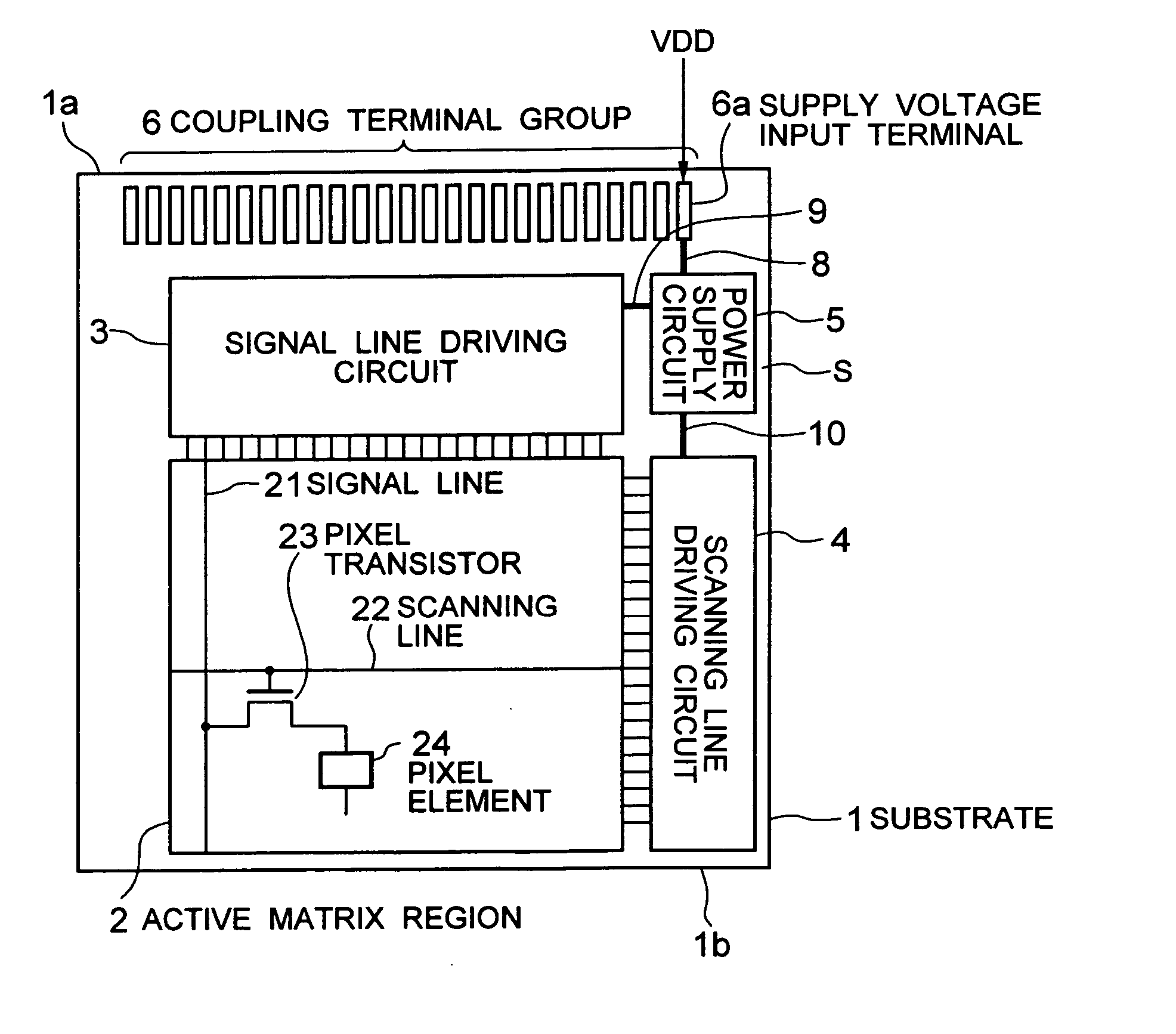
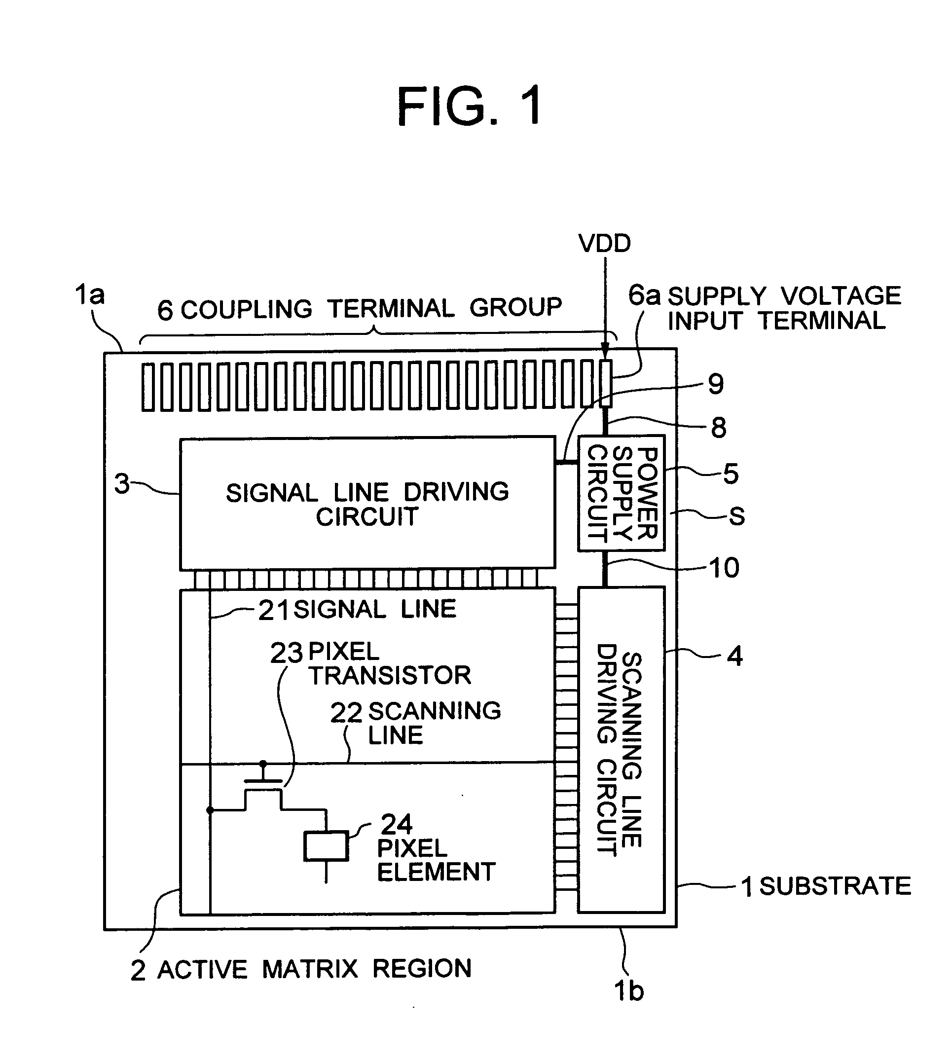
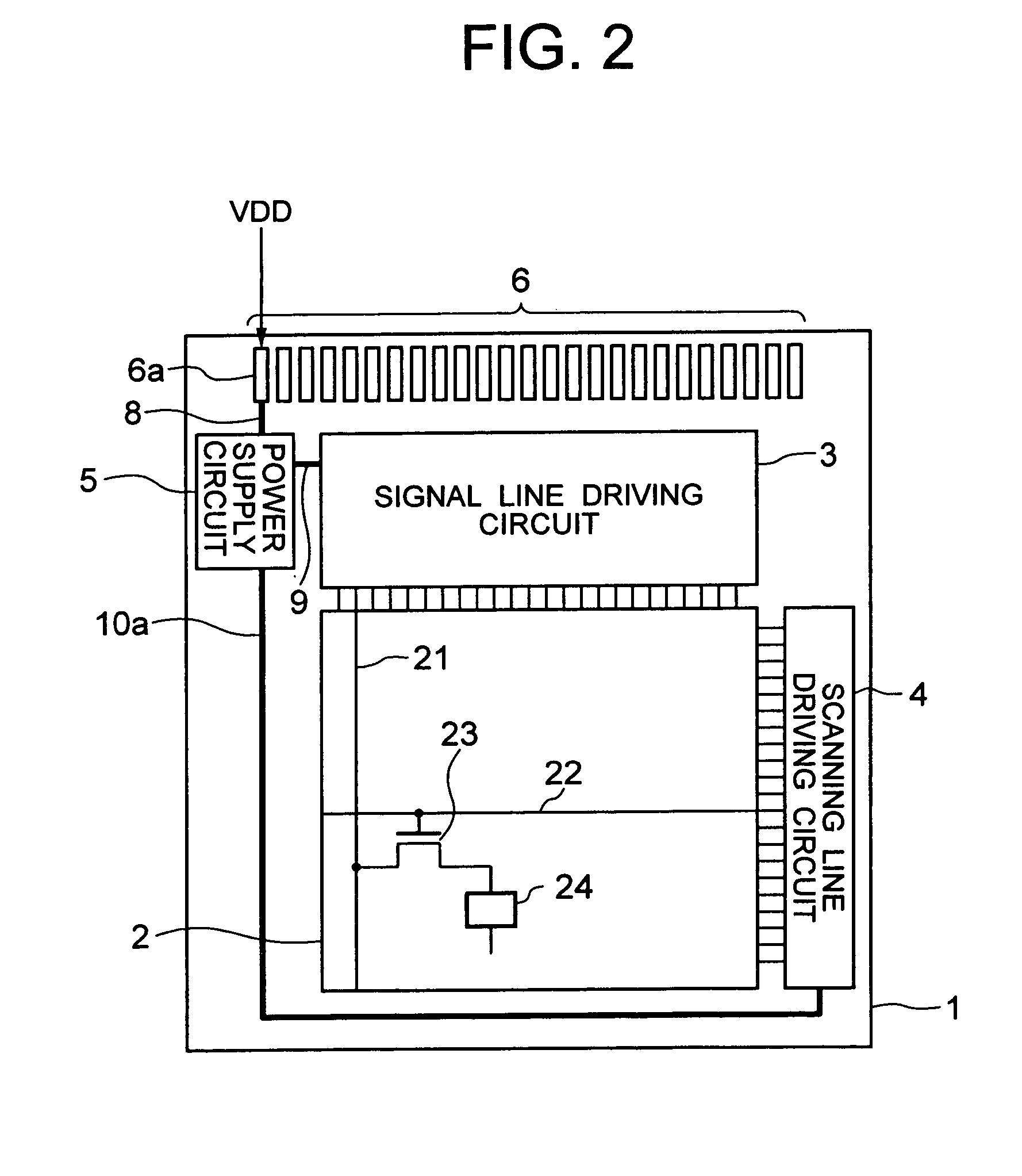
Active matrix type semiconductor device
a semiconductor device and active matrix technology, applied in the direction of identification means, instruments, process and machine control, etc., can solve the problems of inability to supply the stable voltage to the signal line driving circuit, the size of the substrate can be reduced, and the layout area required for power supply wiring becomes large. , to achieve the effect of high-density integrated device, reduced substrate size, and reduced wiring area
- Summary
- Abstract
- Description
- Claims
- Application Information
AI Technical Summary
Benefits of technology
Problems solved by technology
Method used
Image

Examples
example 1
[0080] Next, EXAMPLE 1 of the present invention will be described by referring to the drawings. The semiconductor device of the EXAMPLE is a case of a display device formed on a substrate such as glass.
[0081]FIG. 10 is a circuit diagram for showing EXAMPLE 1 of the semiconductor device according to the present invention. FIG. 11 is a block diagram for showing the power supply circuit shown in FIG. 10. Description will be provided hereinafter by referring to the drawings.
[0082] On a substrate 100, formed are a display unit 101 such as liquid crystal, a signal line driving circuit 102, a scanning line driving circuit 103, a power supply circuit 104 for generating the supply voltage which is used by the above-mentioned components, a signal wiring (the numeral reference is omitted) and power supply wirings 8a, 9a, 10b, 11 for transmitting the signals from outside of the substrate and the supply voltage to the circuits on the substrate 100, a coupling terminal 105 for inputting the sup...
example 2
[0097] Next, EXAMPLE 2 of the present invention will be described by referring to the drawings. The EXAMPLE is a case of a sensor device formed on a substrate such as glass.
[0098]FIG. 15 is a circuit diagram for showing EXAMPLE 2 of the semiconductor device according to the present invention. Description will be provided hereinafter by referring to the drawing. However, the description of the same components as the ones in FIG. 10 will be omitted by applying the same reference numerals.
[0099] On a substrate 100, formed are a sensor unit 110 such as photodiode, a signal line driving circuit 102, a scanning line driving circuit 103, a power supply circuit 104 for generating the supply voltage which is used by the above-mentioned components, a signal wiring (the numeral reference is omitted) and power-supply wirings 8a, 9a, 10b, 11 for transmitting the signals from outside of the substrate 100 and the supply voltage to the circuits on the substrate 100, a coupling terminal 105 for in...
PUM
| Property | Measurement | Unit |
|---|---|---|
| threshold voltage | aaaaa | aaaaa |
| output voltage | aaaaa | aaaaa |
| supply voltage | aaaaa | aaaaa |
Abstract
Description
Claims
Application Information