
Organic electroluminescent device and fabrication method thereof

an electroluminescent device and organic technology, applied in the field of display devices, can solve the problems of significant power consumption and degraded contrast, and achieve the effect of improving the picture quality and improving the brightness of the organic el devi

Active Publication Date: 2005-08-18
LG DISPLAY CO LTD
View PDF13 Cites 29 Cited by
  • Summary
  • Abstract
  • Description
  • Claims
  • Application Information

AI Technical Summary

Benefits of technology

The present invention aims to solve problems in the prior art by providing an organic EL filter with increased overall transmissivity and lowered reflectance, improving luminous efficiency of the panel. Additionally, the invention includes a method of manufacturing the organic electroluminescent device with a front surface panel including a filter to reduce reflection of external light. The invention can significantly improve brightness without reducing contrast and improve picture quality of the organic EL device.

Problems solved by technology

The organic EL display panel is disadvantageous in implementing a large-size screen, but is advantageous in resolution, power consumption, etc., compared with a PDP.
However, this PM type has problems in that the current flowing through respective pixels must be the same so as to make uniform the brightness of the whole pixel, and power consumption is significantly great since the charge / discharge current applied to a capacitive load is high.
Meanwhile, the organic EL panel has reflectance of over 80%, which results in degraded contrast.

Method used


Image

  • Organic electroluminescent device and fabrication method thereof
  • Organic electroluminescent device and fabrication method thereof
  • Organic electroluminescent device and fabrication method thereof

Examples


first embodiment

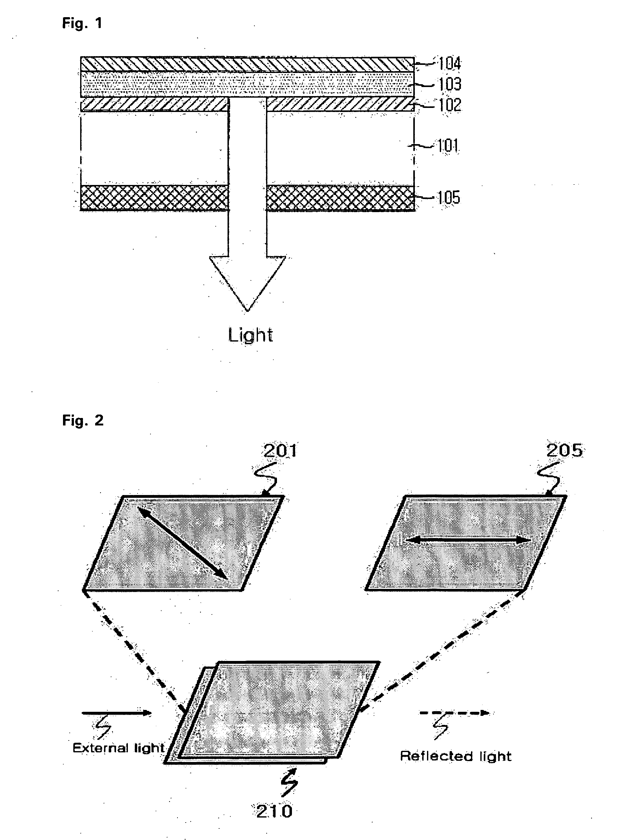
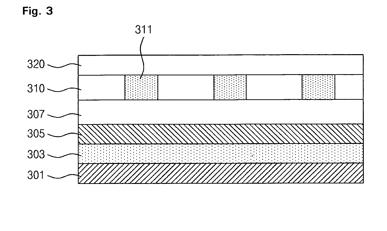
[0063]FIG. 3 is a cross-sectional view illustrating the construction of an organic EL panel to which a filter according to the present invention is applied.

[0064] The organic EL panel includes an anode 305 and a cathode 301 with a phosphor layer 303 interposed therebetween.

[0065] A front electrode layer 305 corresponding to the anode 305, which is located in front of the panel, is generally made of indium tin oxide (ITO). ITO is a thin film material for a transparent electrode, and is coated on the thin film as the transparent electrode by means of a vacuum deposition method, thereby implementing conductivity. Generally, the transmissivity of the front electrode layer 305 is 80% or over.

[0066] The phosphor layer 303 can consist of a RIG / B phosphor layer or a white phosphor layer depending on its light emission mode. If the phosphor layer 303 is composed of the white phosphor layer, a R / G / B color filter is further formed on the anode electrode plate, thereby properly implementing R...

second embodiment

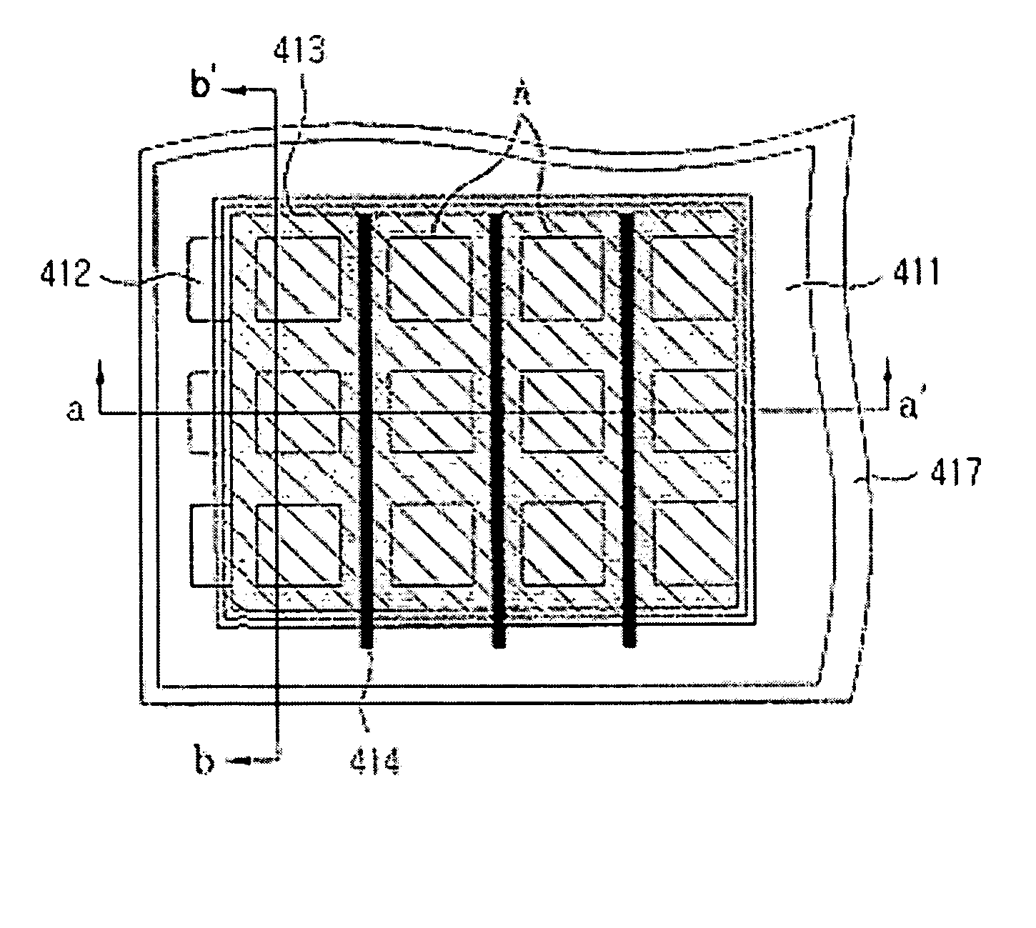
[0103]FIGS. 7a to 7c are views illustrating the construction of an organic electroluminescent device according to the present invention.

[0104] The organic electroluminescent device of a passive type according to the second embodiment of the present invention will be below described with reference to FIG. 7a to 7c.

[0105] Referring first to FIG. 7a, a plurality of anodes 412 made of ITO (Indium Tin Oxide) is formed on a transparent substrate 411 with a given distance therebetween. A black insulating film 413 for providing insulation among pixels is then formed on the entire surface other than pixel (A) portions, which will become light-emitting regions.

[0106] In this time, preferably, the black insulating film 413 covers portions except for the light-emitting regions (pixel portions), and can be patterned in the form of a stripe or matrix.

[0107] Further, the black insulating film 413 can be made of any one of organic material, inorganic material, polymer, inorganic material oxide, ...

third embodiment

[0116]FIG. 9 is a view illustrating the construction of an organic electroluminescent device according to the present invention.

[0117] The construction of the organic electroluminescent device according to this embodiment will now be described with reference to FIG. 9. It is to be noted that the organic electroluminescent device according to this embodiment has the same basic construction as that of the second embodiment except that it is an active type organic electroluminescent device.

[0118] First, a semiconductor layer 522 such as polysilicon, which will be used as an active layer of a thin film transistor, is formed on a transparent substrate 521, and is then patterned.

[0119] A gate insulating film 523 is formed. Next, a gate electrode 524 is deposited and is then patterned.

[0120] Then, an impurity such as boron (B) or phosphor (P) is injected into portions of the semiconductor layer 522, and is then annealed to form a source-drain region 522a-522c of the thin film transistor...


PUM

PropertyMeasurementUnit
voltageaaaaaaaaaa
voltageaaaaaaaaaa
reflectanceaaaaaaaaaa

Abstract

Disclosed herein is a plasma display panel in which afterimage is improved. The plasma display panel according to the present invention includes a panel unit having an upper plate and a lower plate, a frame that supports circuitry, and a conductive material formed between the panel unit and the frame. As such, a conductive material is formed on a bottom surface of a lower plate of a panel. Thus, charges introduced into the lower plate are properly controlled to improve the waveform stability of the panel. Also, a charge characteristic is improved to implement a stable operation. Accordingly, an afterimage time can be reduced. Further, a sheet of a low hardness and light weight is used. It is thus possible to absorb shock and noise of a PDP, accomplish light weight of the PDP and reduce the materials of the sheet.

Description

[0001] This Nonprovisional application claims priority under 35 U.S.C. § 119(a) on Patent Application No. 10-2004-0004461 filed in Korea on Jan. 20, 2004, Patent Application No. 10-2004-0072116 filed in Korea on Sep. 9, 2004, the entire contents of which are hereby incorporated by reference. BACKGROUND OF THE INVENTION [0002] 1. Field of the Invention [0003] The present invention relates to a display device, and more particularly, to an organic electroluminescent (EL) device and a method of manufacturing the same, wherein the picture quality of an organic electroluminescent display (OELD) can be improved. [0004] 2. Description of the Background Art [0005] Recently, as the size of display devices increases, there is an increasing need for flat panel display devices that occupy a smaller area. Electroluminescent (EL) devices have come into the spotlight as one of these flat panel display devices. [0006] The electroluminescent devices can be mainly classified into inorganic electrolumi...

Claims


Application Information

Patent Timeline
Patent Type & Authority Applications(United States)
IPC IPC(8): G02B5/22G02B1/11H01L27/32H01L51/50H01L51/52H05B33/02H05B33/10H05B33/12
CPCH01L27/3244H01L27/3251H01L2251/5315H01L27/3283H01L51/5284H01L27/3281H10K59/127H10K59/17H10K59/173H10K59/12H10K2102/3026H10K59/8792H10K50/865
Inventor RYU, BYUNG GILKIM, KYUNG KUCHA, HONG RAECHANG, MYEONG SOOHAN, YOUNG SOOKIM, HWA KYUNGKYUNG, JAE WOOCHOI, HONG SEOKJUNG, MYUNG JONGKIM, CHANG NAM
Owner LG DISPLAY CO LTD
Learn More