Light emitting device

a light emitting device and active matrix technology, applied in the direction of luminescnet screens, discharge tubes, identification means, etc., can solve the problems of reducing the efficiency of light extraction toward the outside of the light emitting device, affecting the normal operation of transistors, and easy diffusion of impurities on the substrate formed from plastic. to achieve the effect of preventing the diffusion of impurities

Active Publication Date: 2005-08-18
SEMICON ENERGY LAB CO LTD
View PDF19 Cites 55 Cited by
  • Summary
  • Abstract
  • Description
  • Claims
  • Application Information

AI Technical Summary

Benefits of technology

[0009] It is an object of the present invention to provide an active matrix light emitting device which reduces a reflection of light in a process of extracting light toward the outside of the light emitting device and which can sufficiently prevent the diffusion of impurities from a substrate to a transistor.

Problems solved by technology

Due to such reflection of light, light extraction efficiency toward the outside of the light emitting device is reduced.
In addition, when impurities of an alkali metal and the like are attached to a substrate formed from plastic, the substrate formed from plastic easily diffuses impurities.
It is concerned that a transistor does not work normally if the impurities are mixed into the transistor.
However, in the case where the insulating layer for preventing the diffusion of impurities is provided, it is concerned that light is reflected in the interface between the insulating layer and a transparent electrode or in the interface between the insulating layer and the substrate, and thus, light extraction efficiency is reduced as described above.

Method used


Image

  • Light emitting device
  • Light emitting device
  • Light emitting device

Examples


embodiment mode 1

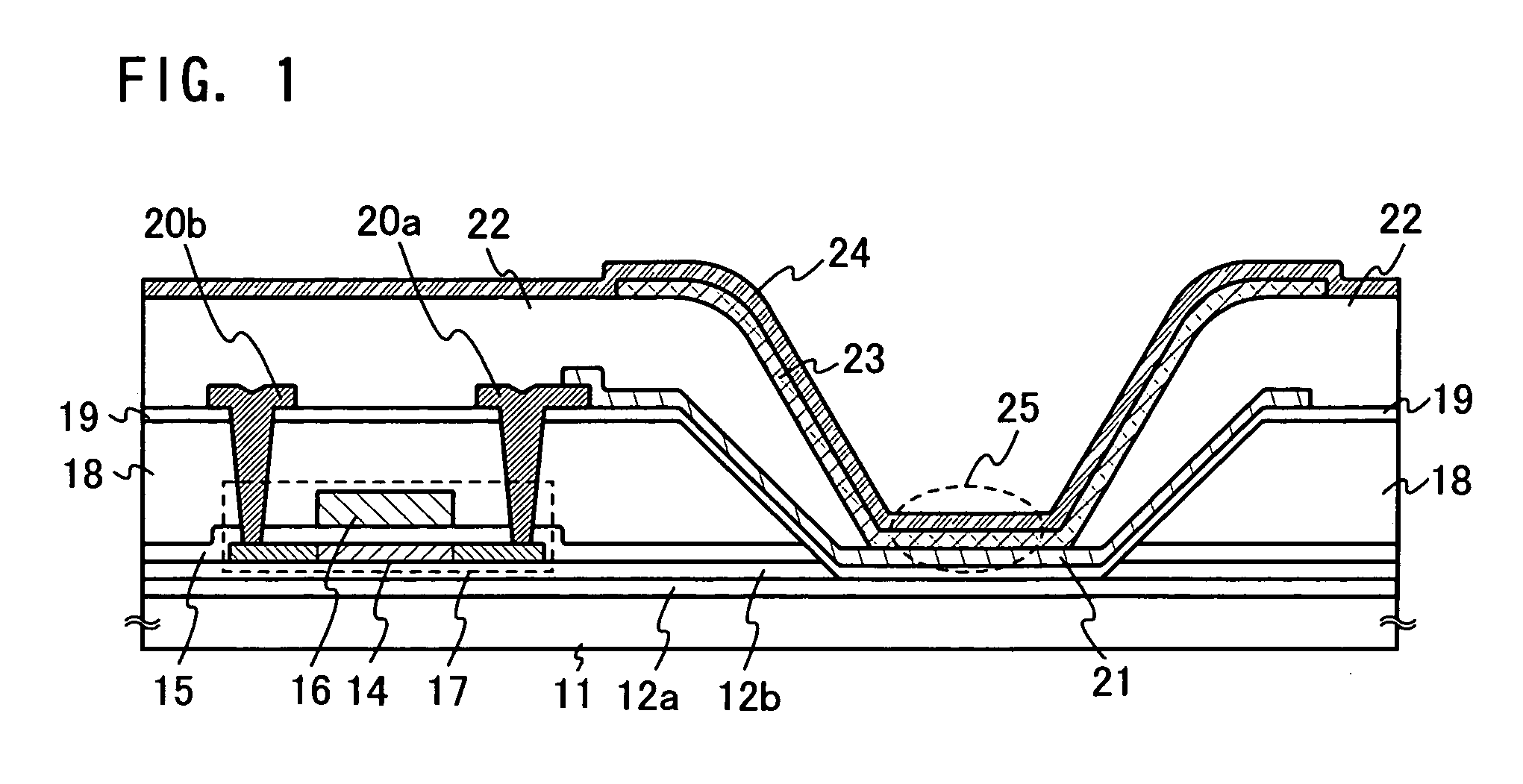
[0037] A light emitting device according to the present invention is described with reference to FIG. 1.

[0038] An insulating layer 12 constituted by two layers of an insulating layer 12a and an insulating layer 12b is provided over a substrate 11. A staggered transistor 17 including a semiconductor layer 14, a gate insulating layer 15 and a gate electrode 16 is provided over the insulating layer 12b.

[0039] The transistor 17 is covered with an insulating layer 18 having a first opening portion. The first opening portion penetrates the gate insulating layer 15 and the insulating layer 12b to reach the insulating layer 12a. Therefore, in the first opening portion, a part of the insulating layer 12a is exposed.

[0040] The insulating layer 18 and the first opening portion are covered with an insulating layer 19, and the insulating layer 19 and the insulating layer 12a are overlapped with each other inside the first opening portion.

[0041] A light emitting element 25 is constituted by a...

embodiment mode 2

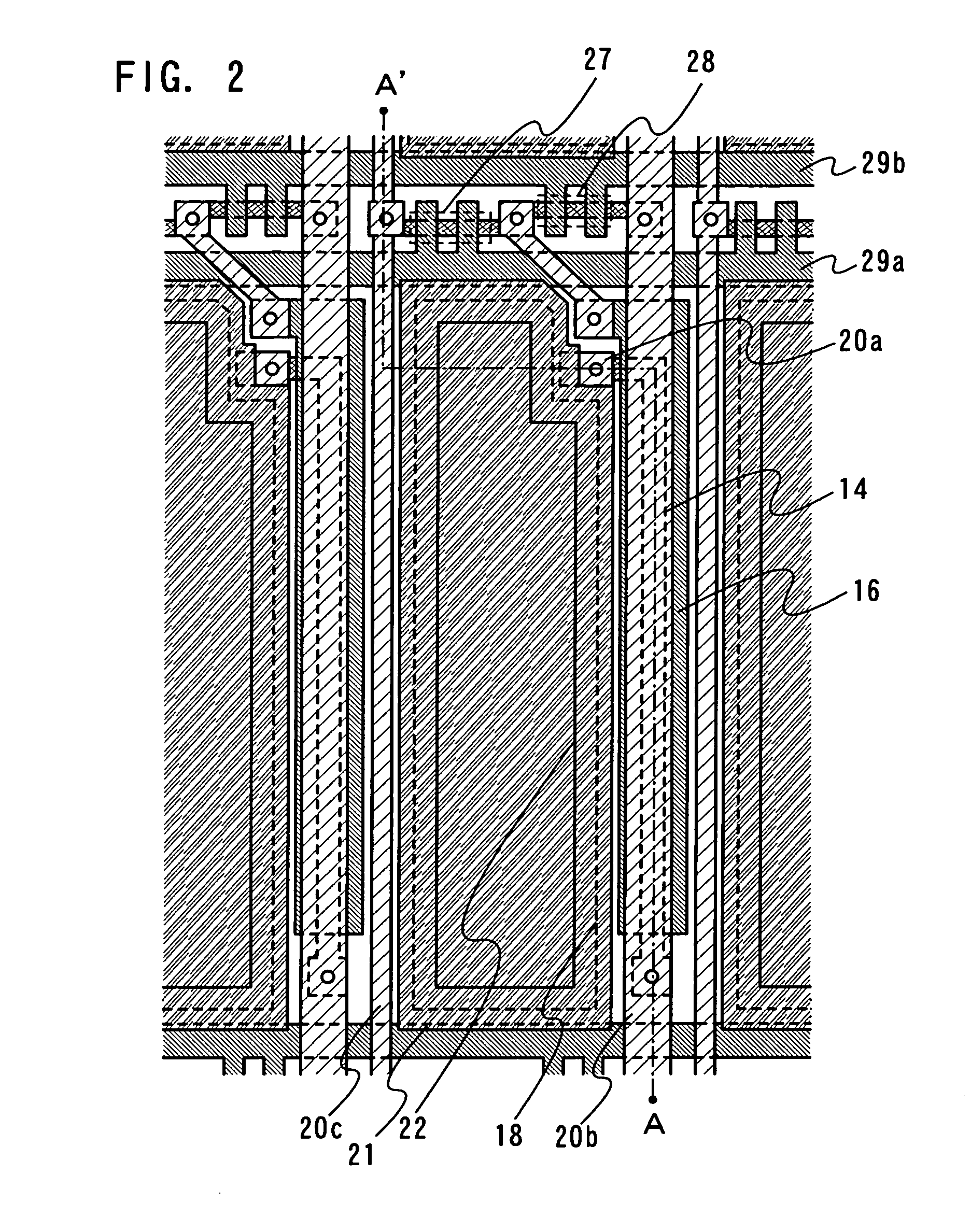
[0055] In this embodiment mode, a method for manufacturing a light emitting device of the present invention shown in FIGS. 1 and 2 is described with reference to FIGS. 3A to 3E and FIGS. 4A to 4D.

[0056] An insulating layer 12a and an insulating layer 12b are sequentially stacked over a substrate 11, and then, a semiconductor layer 14 is stacked over the insulating layer 12b. Further, the insulating layer 12a is preferably formed from silicon nitride containing oxygen. The insulating layer 12a is more preferably a layer formed from silicon nitride containing an oxygen element of from 5% to 6% when Rutherford Back Scattering / Hydrogen Forward Scattering (RBS / HFS) analysis is performed. The layer formed from silicon nitride containing an oxygen element of from 5% to 6% can be formed by using gas as a material in which, for example, monosilane (SiH4), ammonia (NH3), nitrous oxide (N2O), and hydrogen (H2) are mixed so as to have a flow ratio of 1:10:2:40 respectively, by a plasma CVD met...

embodiment mode 3

[0073] In this embodiment mode, a light emitting device of the present invention in which a structure and a method for manufacturing thereof are different from that of the light emitting device in Embodiment Modes 1 and 2 is described with reference to FIGS. 5A to 5E and FIGS. 6A and 6B.

[0074] An insulating layer 52a and an insulating layer 52b are sequentially stacked over a substrate 51, and then, a semiconductor layer 53 is stacked over the insulating layer 52b. Note that the insulating layer 52a is preferably formed from silicon nitride containing oxygen. The insulating layer 52a is more preferably a layer formed from silicon nitride containing an oxygen element of from 5% to 6% when Rutherford Back Scattering / Hydrogen Forward Scattering (RBS / HFS) analysis is performed. The layer formed from silicon nitride containing an oxygen element of from 5% to 6% can be formed by using gas as a material in which, for example, monosilane (SiH4), ammonia (NH3), nitrous oxide (N2O), and hydr...


PUM


Abstract

It is an object of the present invention to provide an active matrix light emitting device which can efficiently prevent a diffusion of impurities from a substrate to a transistor, as well as reducing a reflection of light in a process of extracting light toward the outside of the light emitting device. One feature of the present invention is a light emitting device including a substrate, a first insulating layer provided over the substrate, a transistor provided over the first insulating layer, and a second insulating layer having a first opening portion which is provided to expose the substrate as well as covering the transistor, wherein a light emitting element is provided inside the first opening portion.

Description

BACKGROUND OF THE INVENTION [0001] 1. Field of the Invention [0002] The present invention relates to an active matrix light emitting device. More specifically, the invention relates to a structure of a part from which light is extracted. [0003] 2. Description of the Related Art [0004] A light emitting device utilizing light from an electroluminescent element (a light emitting element) attracts attention as a low power consumption display device having a wide viewing angle. [0005] There are an active matrix type and a passive matrix type as driving methods for a light emitting device mainly used for display. In an active matrix light emitting device, an emission state, a non-emission state or the like of every light emitting element can be controlled. Therefore, an active matrix light emitting device can be driven with lower power consumption than that of a passive matrix light emitting device, and it is suitable for being mounted not only as a display portion of a small electric app...

Claims


Application Information

Patent Timeline
Patent Type & Authority Applications(United States)
IPC IPC(8): G09F9/30H01L27/32H01L51/52H05B33/00H05B33/02H05B33/12H05B33/22
CPCH01L27/3246H01L51/5262H01L27/3258H01L27/3248H10K59/123H10K59/124H10K59/122H10K59/875H10K50/85
Inventor KAWAKAMI, TAKAHIROTSUCHIYA, KAORUNISHI, TAKESHIHIRAKATA, YOSHIHARUKIDA, KEIKOSATO, AYUMIYAMAZAKI, SHUNPEI
Owner SEMICON ENERGY LAB CO LTD
Why Eureka
Try Eureka