
Preparation of halftone phase shift mask blank

Active Publication Date: 2005-08-25
SHIN ETSU CHEM CO LTD
View PDF3 Cites 11 Cited by
  • Summary
  • Abstract
  • Description
  • Claims
  • Application Information

AI Technical Summary

Benefits of technology

[0014] Therefore, an object of the present invention is to provide a method for preparing a halftone phase shift mask blank of consistent quality which has a minimized variation of transmittance and less defects; a halftone phase shift mask blank; a halftone phase shift mask; and a pattern transfer method using the mask.
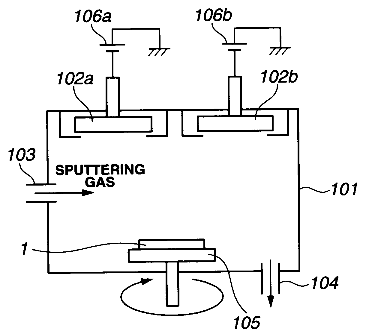
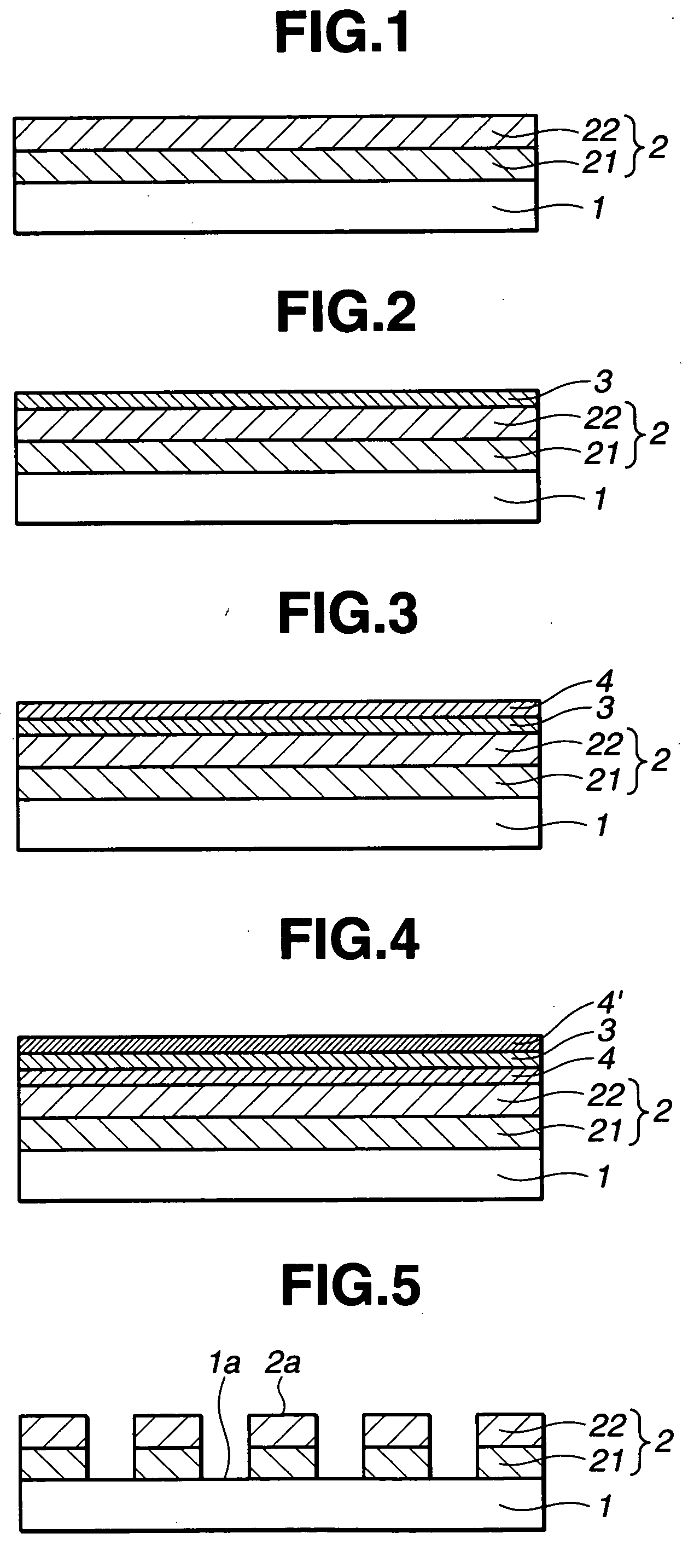
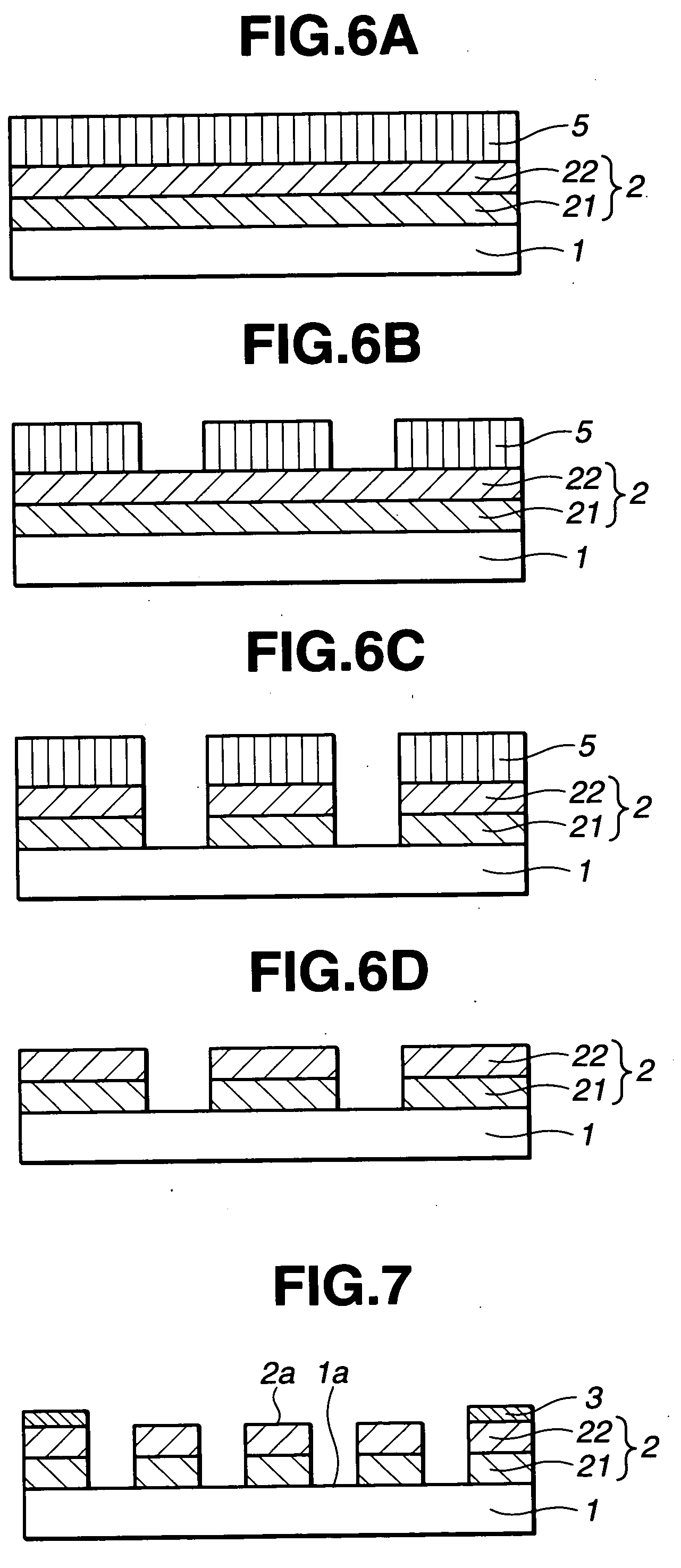
[0015] The present invention addresses a method for preparing a halftone phase shift mask blank, in which a halftone phase shift film containing at least one layer of metal and silicon-containing compound film is formed on a transparent substrate by a co-sputtering process including the steps of disposing (A) a metal-containing target and (B) a silicon target in a chamber, feeding a sputtering gas into the chamber, applying electric powers across the targets (A) and (B) at the same time to produce an electric discharge for sputtering. The inventor has discovered that when the area of the sputtered region of the metal-containing target (A) is smaller than the area of the sputtered region of the silicon target (B), a metal and silicon-containing compound film having a low metal content, especially suited for short wavelength light exposure, can be formed from the high density targets which will release few of the particles that can incur film defects. Since the area of the sputtered region of the metal-containing target is smaller, the sputtering power applied across the metal-containing target can be reduced without lowering the sputtering power density thereat. Then, even when a halftone phase shift film containing a metal and silicon in a low metal / silicon ratio is to be deposited, stable deposition by sputtering becomes possible. This enables to prepare a halftone phase shift mask blank and a halftone phase shift mask of consistent quality which have a minimized variation of transmittance and less defects and which are especially suited for short wavelength light exposure. This halftone phase shift mask allows for pattern transfer to a photoresist through short wavelength light exposure. The invention is predicated on these findings.
[0021] The present invention enables to deposit a film containing a metal and silicon in a low metal / silicon ratio at a consistent level of quality without lowering the sputtering power density at the metal-containing target and while restraining particles from being released from the targets. There are thus provided a halftone phase shift mask blank and a halftone phase shift mask of consistent quality which are especially suited for short wavelength light exposure.

Problems solved by technology

This lowers the process stability and adversely affects the manufacture yield of products.
Several problems arise with the metal silicide target having a low metal content.
This fails to produce a target having a satisfactory sintered density.
If a target having an unsatisfactory sintered density is used in the deposition of a halftone phase shift film, there can arise a problem that particles are released from the target during sputter deposition, resulting in increased film defects.
In depositing a halftone phase shift film containing metal and silicon in such a lower metal / silicon ratio, the co-sputtering process encounters a problem that the sputtering power applied across the target having a high metal content (e.g., MoSi2 target) largely differs from the sputtering power applied across the target having a low metal content (e.g., single crystal silicon target), that is, there is a significant difference in power density (W / cm2) between these targets.
Since it is impossible to apply powers to both the targets at optimum power densities, the composition within the halftone phase shift film being deposited becomes inconsistent, leading to large variations of transmittance.
The electric discharge of sputtering also becomes unstable, sometimes resulting in even increased film defects.

Method used


Image

  • Preparation of halftone phase shift mask blank
  • Preparation of halftone phase shift mask blank
  • Preparation of halftone phase shift mask blank

Examples


example 1

[0064] The sputtering targets used were a sintered MoSi2 target having a sputter region with an area of 150 cm2 and a single crystal Si target having a sputter region with an area of 310 cm2.

[0065] First, a light absorption function film was deposited on a quartz substrate. As the sputtering gas, Ar, N2 and O2 gases were fed to the chamber at a flow rate of 20 cm3 / min, 10 cm3 / min and 4 cm3 / min, respectively. During the gas feed, a gas pressure of 0.10 Pa was set in the sputtering chamber. By applying a sputtering power of 200 W across the sintered MoSi2 target and a sputtering power of 1300 W across the single crystal Si target for co-sputtering and rotating the substrate at 30 rpm, a light absorption function film (MoSiON film) was deposited to a thickness of 5.0 nm. The MoSiON film had the composition: 7 at % Mo, 52 at % Si, 20 at % O, and 21 at % N.

[0066] Next, a phase shift function film was deposited. Deposition was performed under the same conditions as used for the light ab...

example 2

[0070] The sputtering targets used were a metal Mo target having a sputter region with an area of 50 cm2 and a single crystal Si target having a sputter region with an area of 310 cm2.

[0071] First, a light absorption function film was deposited on a quartz substrate. As the sputtering gas, Ar, N2 and O2 gases were fed to the chamber at a flow rate of 20 cm3 / min, 10 cm3 / min and 4cm3 / min, respectively. During the gas feed, a gas pressure of 0.10 Pa was set in the sputtering chamber. By applying a sputtering power of 70 W across the Mo target and a sputtering power of 1300 W across the single crystal Si target for co-sputtering and rotating the substrate at 30 rpm, a light absorption function film (MoSiON film) was deposited to a thickness of 5.0 nm. The MoSiON film had the composition: 7 at % Mo, 52 at % Si, 20 at % O, and 21 at % N.

[0072] Next, a phase shift function film was deposited. Deposition was performed under the same conditions as used for the light absorption function fil...


PUM

PropertyMeasurementUnit
Ratioaaaaaaaaaa
Areaaaaaaaaaaa
Molar ratioaaaaaaaaaa

Abstract

In preparing a halftone phase shift mask blank, a metal and silicon-containing compound film serving as a halftone phase shift film is formed on a transparent substrate by a co-sputtering process including the steps of disposing a metal-containing target and a silicon target in a chamber, feeding sputtering gases into the chamber, and applying electric powers across both the targets at the same time. The sputtered region area of the metal-containing target is smaller than the sputtered region area of the silicon target.

Description

CROSS-REFERENCE TO RELATED APPLICATION [0001] This non-provisional application claims priority under 35 U.S.C. §119(a) on Patent Application No. 2004-042990 filed in Japan on Feb. 19, 2004, the entire contents of which are hereby incorporated by reference. TECHNICAL FIELD [0002] This invention relates to a halftone phase shift mask blank and halftone phase shift mask for use in the fabrication of semiconductor integrated circuits or the like. More particularly, it relates to a method for preparing a halftone phase shift mask blank, a halftone phase shift mask blank prepared thereby, a halftone phase shift mask obtained therefrom, and a pattern transfer method using the same. BACKGROUND ART [0003] Photomasks are used in a wide variety of applications including the fabrication of semiconductor integrated circuits such as ICs, LSIs and VLSIs. Basically, the photomask is prepared from a photomask blank having a chromium based light-shielding film on a transparent substrate, by forming a...

Claims


Application Information

Patent Timeline
IPC IPC(8): C23C14/00C23C14/06C23C14/32C23C14/34G03C5/00G03F1/32G03F1/54G03F1/68G03F9/00H01L21/027
CPCC23C14/0676G03F1/54G03F1/32C23C14/3464G03F1/26
Inventor YOSHIKAWA, HIROKIOKAZAKI, SATOSHI
Owner SHIN ETSU CHEM CO LTD
Learn More