Barrier film material and pattern formation method using the same

a barrier film and film material technology, applied in the direction of photosensitive materials, instruments, photomechanical equipment, etc., can solve the problems of reducing the productivity and yield of the semiconductor device fabrication process, and achieve the effect of improving the dissolution characteristic of the resist and good shap

Inactive Publication Date: 2005-08-25
RPX CORP
View PDF9 Cites 27 Cited by
  • Summary
  • Abstract
  • Description
  • Claims
  • Application Information

AI Technical Summary

Benefits of technology

[0038] The second pattern formation method using the barrier film material of this invention includes the steps of forming a resist film made of a chemically amplified resist on a substrate; forming a barrier film on the resist film; performing pattern exposure by selectively irradiating the resist film with exposing light with a liquid provided on the barrier film; and removing the barrier film and forming a resist pattern made of the resist film by developing the resist film after the pattern exposure, and the barrier film prevents a component of the resist film from eluting into the liquid or prevents the liquid from permeating into the resist film.
[0039] In the second pattern formation method, the barrier film formed on the resist film prevents a component of the resist film from eluting into the liquid or prevents the liquid from permeating into the resist film in the same manner as in the first pattern formation method, and therefore, the resist film keeps the expected performance of the chemically amplified resist during the pattern exposure. As a result, the resist pattern made of the resist film can be formed in a good shape.
[0040] A difference between the first pattern formation method and the second pattern formation method is that the barrier film formed on the resist film is removed before the development in the first pattern formation method while it is removed during the development with a developer in the second pattern formation method. In the case of the first pattern formation method, since the barrier film is removed before the development, the development processing is generally proceeded. Alternatively, in the case of the second pattern formation method, since the barrier film is removed during the development, the dissolution characteristic of the resist can be controlled, resulting in improving the dissolution characteristic of the resist. The control of the dissolution characteristic will be described later.

Problems solved by technology

In either case, when the resist pattern 2a in such a defective shape is used for etching a target film, the resultant pattern of the target film is also in a defective shape, which disadvantageously lowers the productivity and the yield in the fabrication process for semiconductor devices.

Method used


Image

  • Barrier film material and pattern formation method using the same
  • Barrier film material and pattern formation method using the same
  • Barrier film material and pattern formation method using the same

Examples


embodiment 1

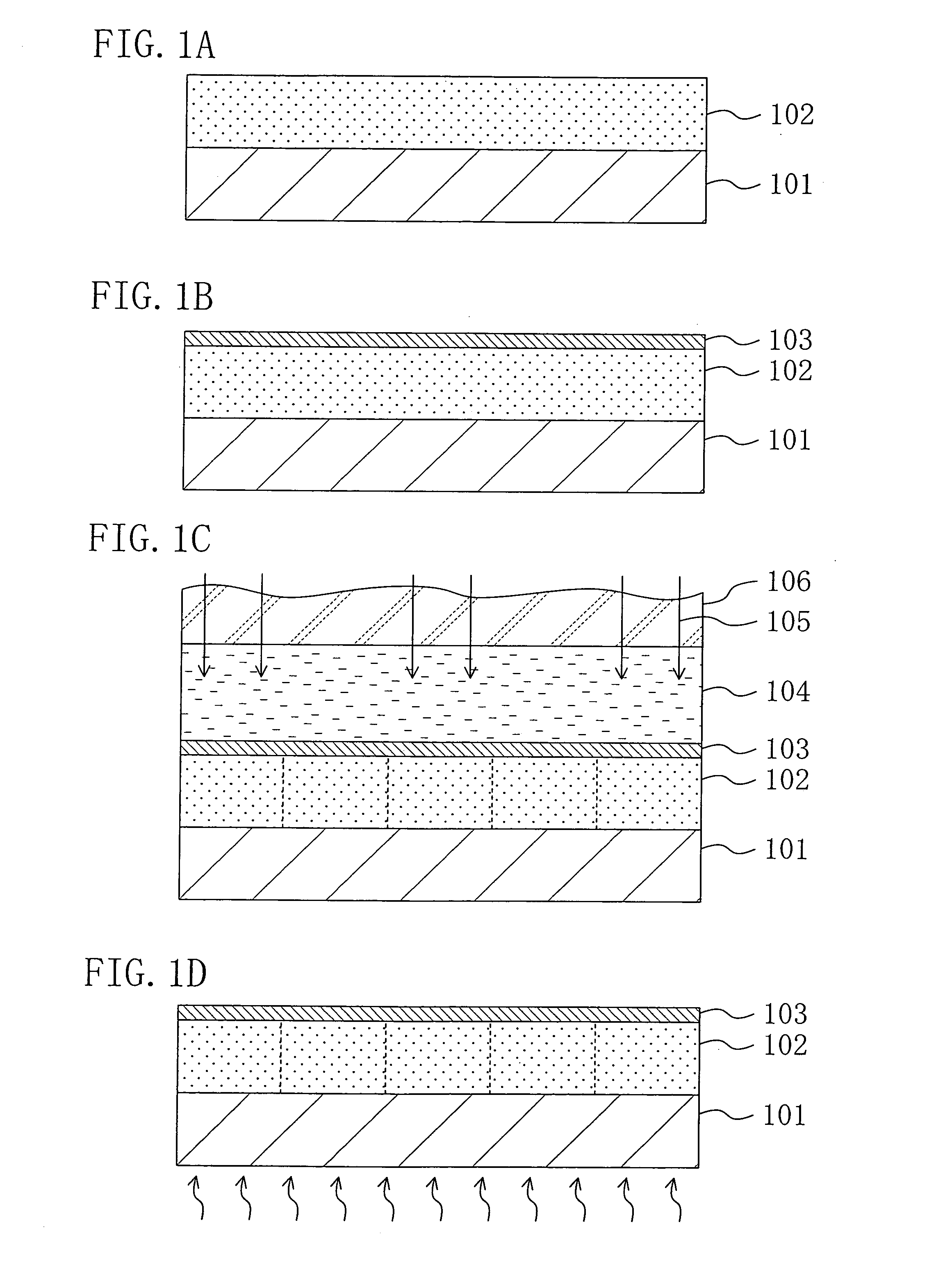
[0068] A pattern formation method using a barrier film material according to Embodiment 1 of the invention will now be described with reference to FIGS. 1A through 1D, 2A and 2B.

[0069] First, a positive chemically amplified resist material having the following composition is prepared: [0070] Base polymer: poly((norbornene-5-methylene-t-butylcarboxylate) (50 mol %)-(maleic anhydride) (50 mol %)) . . . 2 g [0071] Acid generator: triphenylsulfonium triflate . . . 0.06 g [0072] Quencher: triethanolamine . . . 0.002 g [0073] Solvent: propylene glycol monomethyl ether acetate . . . 20 g

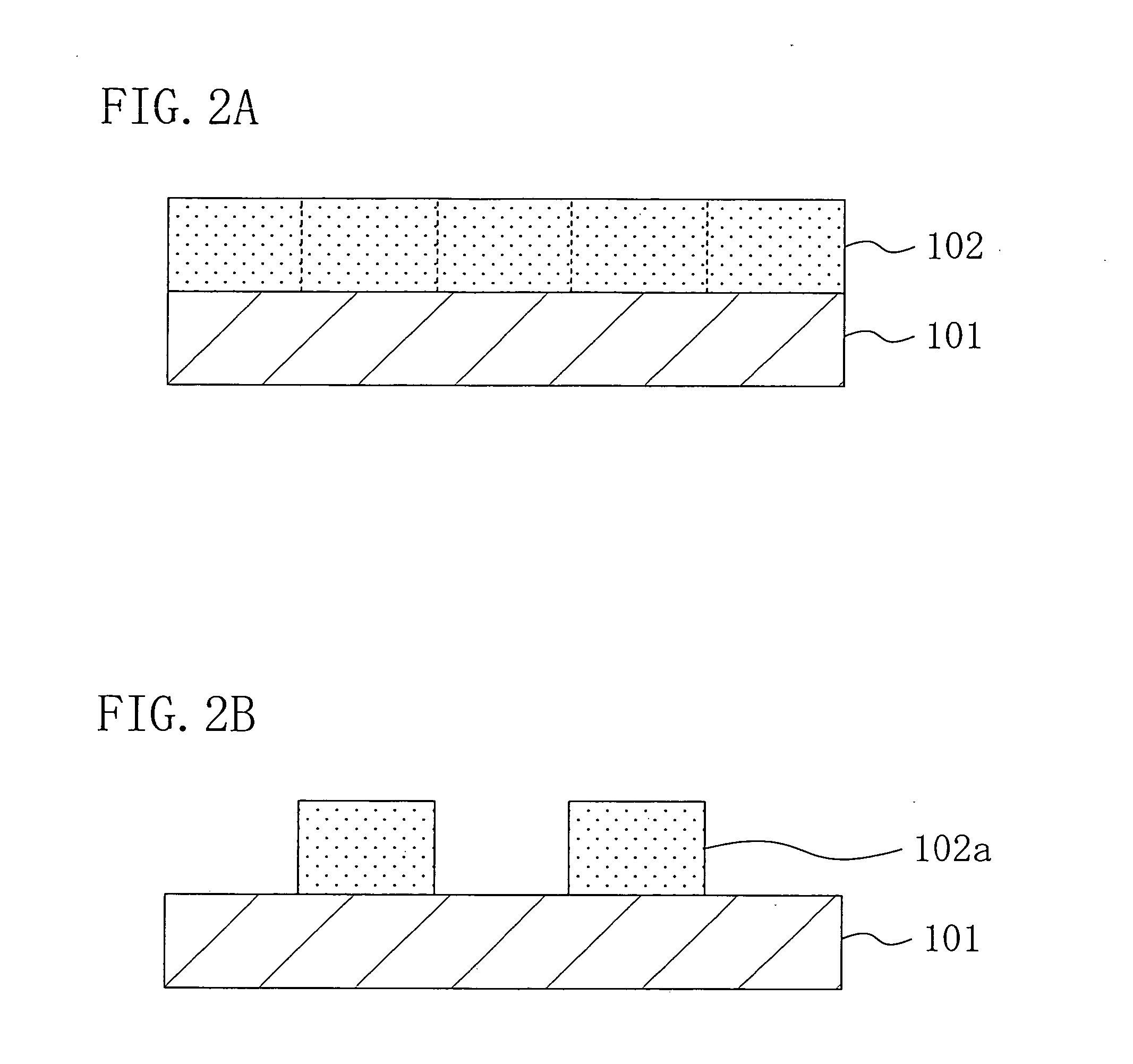
[0074] Next, as shown in FIG. 1A, the aforementioned chemically amplified resist material is applied on a substrate 101 so as to form a resist film 102 with a thickness of 0.35 μm.

[0075] Then, as shown in FIG. 1B, a barrier film 103 that is made of a barrier film material having the following composition, has a thickness of 0.06 μm and is different in its solubility depending upon the value of pH is form...

embodiment 2

[0083] A pattern formation method using a barrier film material according to Embodiment 2 of the invention will now be described with reference to FIGS. 3A through 3D and 4A through 4C.

[0084] First, a positive chemically amplified resist material having the following composition is prepared: [0085] Base polymer: poly((norbornene-5-methylene-t-butylcarboxylate) (50 mol %)-(maleic anhydride) (50 mol %)) . . . 2 g [0086] Acid generator: triphenylsulfonium triflate . . . 0.06 g [0087] Quencher: triethanolamine . . . 0.002 g [0088] Solvent: propylene glycol monomethyl ether acetate . . . 20 g

[0089] Next, as shown in FIG. 3A, the aforementioned chemically amplified resist material is applied on a substrate 201 so as to form a resist film 202 with a thickness of 0.35 μm.

[0090] Then, as shown in FIG. 3B, a barrier film 203 that is made of a barrier film material having the following composition, has a thickness of 0.07 μm and is different in its solubility depending upon the value of pH ...

embodiment 3

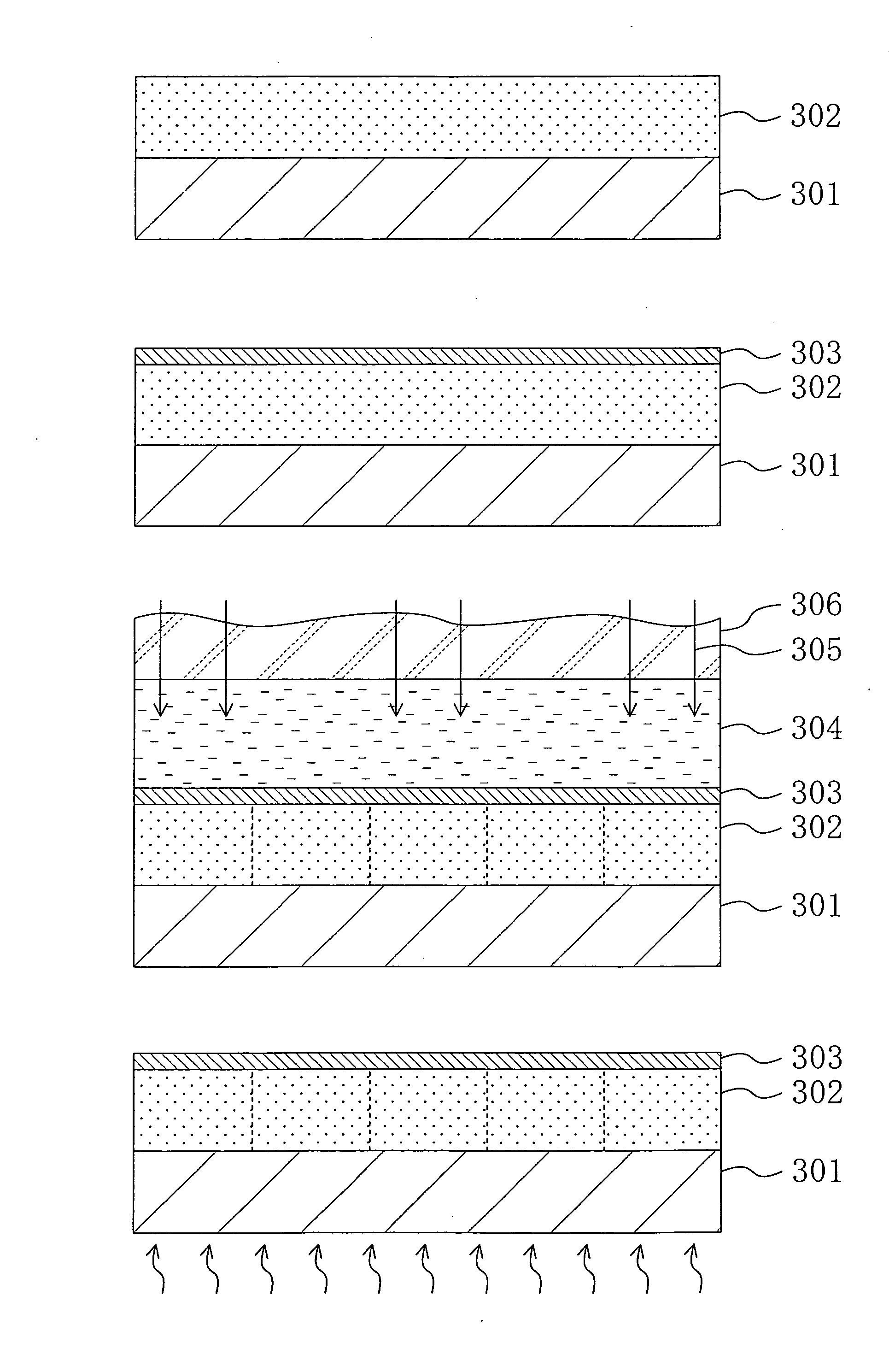
[0100] A pattern formation method using a barrier film material according to Embodiment 3 of the invention will now be described with reference to FIGS. 5A through 5D and 6.

[0101] First, a positive chemically amplified resist material having the following composition is prepared: [0102] Base polymer: poly((norbornene-5-methylene-t-butylcarboxylate) (50 mol %)-(maleic anhydride) (50 mol %)) . . . 2 g [0103] Acid generator: triphenylsulfonium triflate . . . 0.06 g [0104] Quencher: triethanolamine . . . 0.002 g [0105] Solvent: propylene glycol monomethyl ether acetate . . . 20 g

[0106] Next, as shown in FIG. 5A, the aforementioned chemically amplified resist material is applied on a substrate 301 so as to form a resist film 302 with a thickness of 0.35 μm.

[0107] Then, as shown in FIG. 5B, a barrier film 303 that is made of a barrier film material having the following composition, has a thickness of 0.05 μm and is different in its solubility depending upon the value of pH is formed on...


PUM

PropertyMeasurementUnit
thicknessaaaaaaaaaa
temperatureaaaaaaaaaa
widthaaaaaaaaaa

Abstract

A resist film made of a chemically amplified resist is formed on a substrate. Subsequently, a barrier film for preventing a component of the resist film from eluting into an immersion liquid or preventing the immersion liquid from permeating into the resist film is formed on the resist film. Thereafter, with an immersion liquid provided on the barrier film, pattern exposure is carried out by selectively irradiating the resist film with exposing light through the barrier film. Then, after removing the barrier film, the resist film having been subjected to the pattern exposure is developed, so as to form a resist pattern made of the resist film.

Description

CROSS-REFERENCE TO RELATED APLICATIONS [0001] This application claims priority under 35 U.S.C. §119 on Patent Application No. 2004-49323 filed in Japan on Feb. 25, 2004, and Patent Application No. 2004-361058 filed in Japan on Dec. 14, 2004, the entire contents of which are hereby incorporated by reference. BACKGROUND OF THE INVENTION [0002] The present invention relates to a material for a barrier film formed on a resist film for use in fabrication process or the like for semiconductor devices and a pattern formation method using the same. [0003] In accordance with the increased degree of integration of semiconductor integrated circuits and downsizing of semiconductor devices, there are increasing demands for further rapid development of lithography technique. Currently, pattern formation is carried out through photolithography using exposing light of a mercury lamp, KrF excimer laser, ArF excimer laser or the like, and use of F2 laser lasing at a shorter wavelength is being examin...

Claims


Application Information

Patent Timeline
Patent Type & Authority Applications(United States)
IPC IPC(8): G03C5/00G03F7/00G03F7/09G03F7/11G03F7/20H01L21/00H01L21/027H01L21/84
CPCG03F7/11G03F7/70341G03F7/2041Y10S430/123Y10S430/119
Inventor ENDO, MASAYUKISASAGO, MASARU
Owner RPX CORP
Why Eureka
Try Eureka