Current drive circuit and display device using same, pixel circuit, and drive method

a drive circuit and display device technology, applied in static indicating devices, instruments, basic electric elements, etc., can solve the problems of difficult to realize a large sized, inconvenient use of single crystalline silicon substrates for the formation of active elements, and inability to use single crystalline silicon substrates for active elements, etc., to achieve convenient and free brightness adjustment of display devices, the effect of increasing the drive current of light emitting elements

Inactive Publication Date: 2005-09-01
SONY CORP
View PDF8 Cites 127 Cited by
  • Summary
  • Abstract
  • Description
  • Claims
  • Application Information

AI Technical Summary

Benefits of technology

[0034] In this way, by changing the timing of the extinguishing signal, it is possible to conveniently and freely change the brightness of the display device. If the second scanning line is divided into colors of R, G, and B and separately controlled, adjustment of the color balance is also easy.
[0035] Further, where it is desired to obtain the same time average brightness, the drive current of a light emitting element OLED can be made larger by reducing the ratio of the light emitting period (duty).

Problems solved by technology

The former is simple in structure, but makes it difficult to realize a large sized, high definition display, so the active matrix method is being vigorously developed.
Due to this, it becomes relatively large in size.
Due to restrictions of cost and manufacturing facilities, a usage of a single crystalline silicon substrate for the formation of the active elements is not practical.
However, the amorphous silicon and polysilicon used for the formation of the TFT have a worse crystallinity in comparison with single crystalline silicon and have a poor controllability of the conduction mechanism, therefore it has been known that there is a large variation in characteristics in formed TFTs.
Particularly, when a polysilicon TFT is formed on a relatively large sized glass substrate, usually the laser annealing method is used as mentioned above in order to avoid the problem of thermal deformation of the glass substrate, but it is difficult to uniformly irradiate laser energy to a large glass substrate.
As a result, according to equation (1) described above, the current Ids flowing through the OLEDs will largely vary for every pixel and consequently become completely off from the intended value, so a high quality of image cannot be expected as the display.
A similar thing can be said for not only the Vth, but also the variation of parameters of equation (1) such as the carrier mobility μ. Further, a certain degree of fluctuation in the above parameters is unavoidable not only due to the variation among pixels as mentioned above, but also variations for every manufacturing lot or every product.
Not only is this impractical in the mass production process of displays, but it is also extremely difficult to devise countermeasures for fluctuations in characteristics of the TFTs due to the ambient temperature and changes of the TFT characteristics occurring due to usage over a long period of time.

Method used


Image

  • Current drive circuit and display device using same, pixel circuit, and drive method
  • Current drive circuit and display device using same, pixel circuit, and drive method
  • Current drive circuit and display device using same, pixel circuit, and drive method

Examples


Embodiment Construction

[0063] Below, embodiments of the present invention will be explained by referring to the attached drawings.

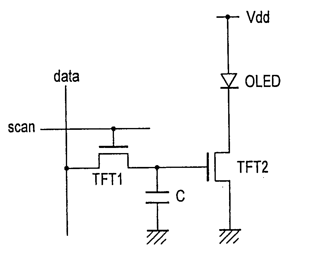
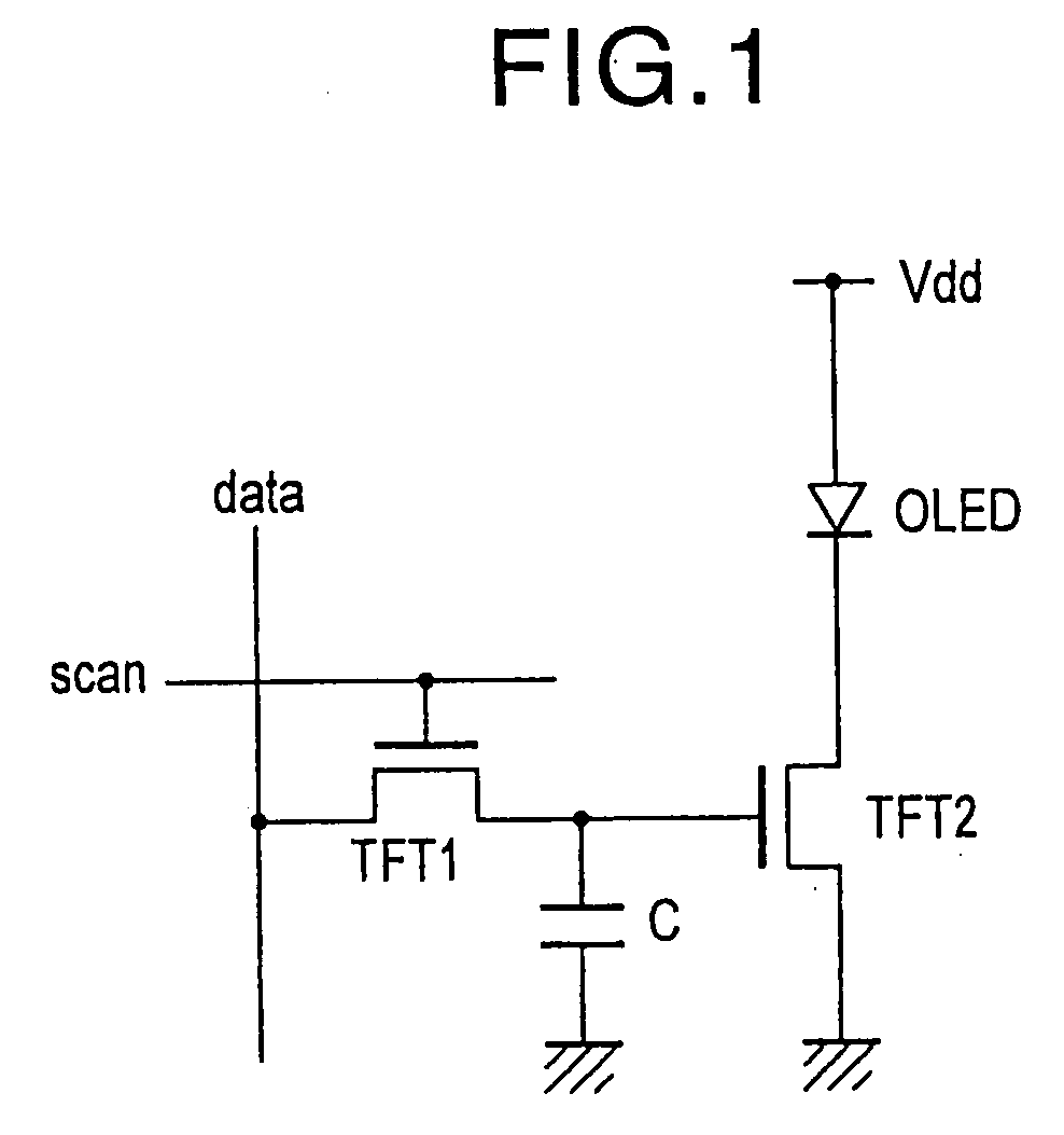
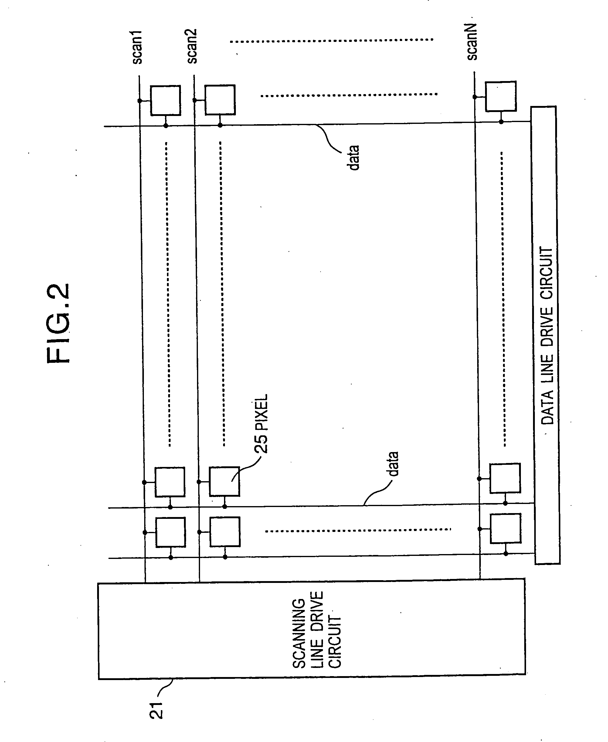
[0064]FIG. 5 shows an example of a pixel circuit according to the present invention. This circuit comprises, other than the conversion use transistor TFT1 with the signal current flowing therethrough and the drive use transistor TFT2 for controlling the drive current flowing through a light emitting element made of an organic EL element or the like, a fetch use transistor TFT3 for connecting or disconnecting the pixel circuit and the data line DATA by the control of a first scanning line SCAN-A, a switch use transistor TFT4 for short-circuiting the gate and the drain of the TFT1 during the writing period by the control of a second scanning line SCAN-B, a capacitor C for holding the voltage between the gate and source of the TFT1 even after the end of the writing, and the light emitting element OLED. In FIG. 5, TFT3 is configured by a PMOS, and the other transistors are configu...


PUM


Abstract

A display device including a current drive circuit capable of stably and correctly supplying an intended current to a light emitting element of each pixel without being affected by variations in characteristics of an active element inside the pixel and as a result capable of displaying a high quality image, wherein each pixel comprises a receiving use transistor TFT3 for fetching a signal current Iw from a data line DATA when a scanning line SCAN-A is selected, a conversion use transistor TFT1 for once converting a current level of a fetched signal current Iw to a voltage level and holding the same, and a drive use transistor TFT2 for passing a drive current having a current level in accordance with the held voltage level through a light emitting element OLED. The conversion use thin film transistor TFT1 generates a converted voltage level at its own gate by passing the signal current Iw fetched by the TFT3 through its own channel. A capacitor C holds the voltage level created at the gate of the TFT1. The TFT2 passes the drive current having a current level in accordance with the held voltage level through the light emitting element OLED.

Description

TECHNICAL FIELD [0001] The present invention relates to a current drive circuit for driving an organic electroluminescence (EL) element or other light emitting element controlled in brightness by a current, a display device providing a light emitting element driven by this current drive circuit for every pixel, a pixel circuit, and a method for driving a light emitting element. In more detail, the present invention relates to a current drive circuit for controlling an amount of the current supplied to a light emitting element by an insulating gate type field effect transistor or other active element provided in each pixel and a so-called active matrix type image display device using the same. BACKGROUND ART [0002] In general, in an active matrix type image display device, an image is displayed by arranging a large number of pixels in a matrix and controlling a light intensity for every pixel in accordance with given brightness information. When using a liquid crystal as an electro-o...

Claims


Application Information

Patent Timeline
Patent Type & Authority Applications(United States)
IPC IPC(8): G09G3/10G09G3/20G09G3/32G09G5/00H01L27/32H05B37/00
CPCG09G3/2014H01L27/3244G09G3/325G09G3/3266G09G2300/0814G09G2300/0842G09G2300/0852G09G2300/0861G09G2300/0866G09G2310/0248G09G2310/0262G09G2320/0223G09G2320/0233G09G2320/0238G09G2320/0242G09G2320/043G09G3/3241H10K59/12
Inventor YUMOTO, AKIRA
Owner SONY CORP
Why Eureka
Try Eureka