IGBT module

a technology of insulated gate bipolar transistor and module, which is applied in the direction of electrical apparatus, semiconductor devices, semiconductor/solid-state device details, etc., can solve the problems of gate voltage oscillation problem, short-circuit current disadvantageously increase, and igbt performance degradation, etc., to achieve significant increase in switching loss and suppress gate voltage oscillation

Inactive Publication Date: 2005-09-08
MITSUBISHI ELECTRIC CORP
View PDF1 Cites 16 Cited by
  • Summary
  • Abstract
  • Description
  • Claims
  • Application Information

AI Technical Summary

Benefits of technology

[0009] It is an object of the present invention to provide an IGBT module capable of suppressing gate voltage oscillation without significantly increasing switching loss.

Problems solved by technology

However, with such miniaturization being advanced further, a short-circuit current disadvantageously increases, and recently, such increase in a short-circuit current (that is, increase in transfer characteristic) has raised the problem of gate voltage oscillation.
In the case of decreasing a saturation current value, however, IGBTs are degraded in performance.
However, increase in gate resistance value decreases the switching speed, which increases switching loss.
In such cases, a gate resistance value increases accordingly, which disadvantageously results in significant increase in switching loss.

Method used


Image

  • IGBT module
  • IGBT module
  • IGBT module

Examples


first preferred embodiment

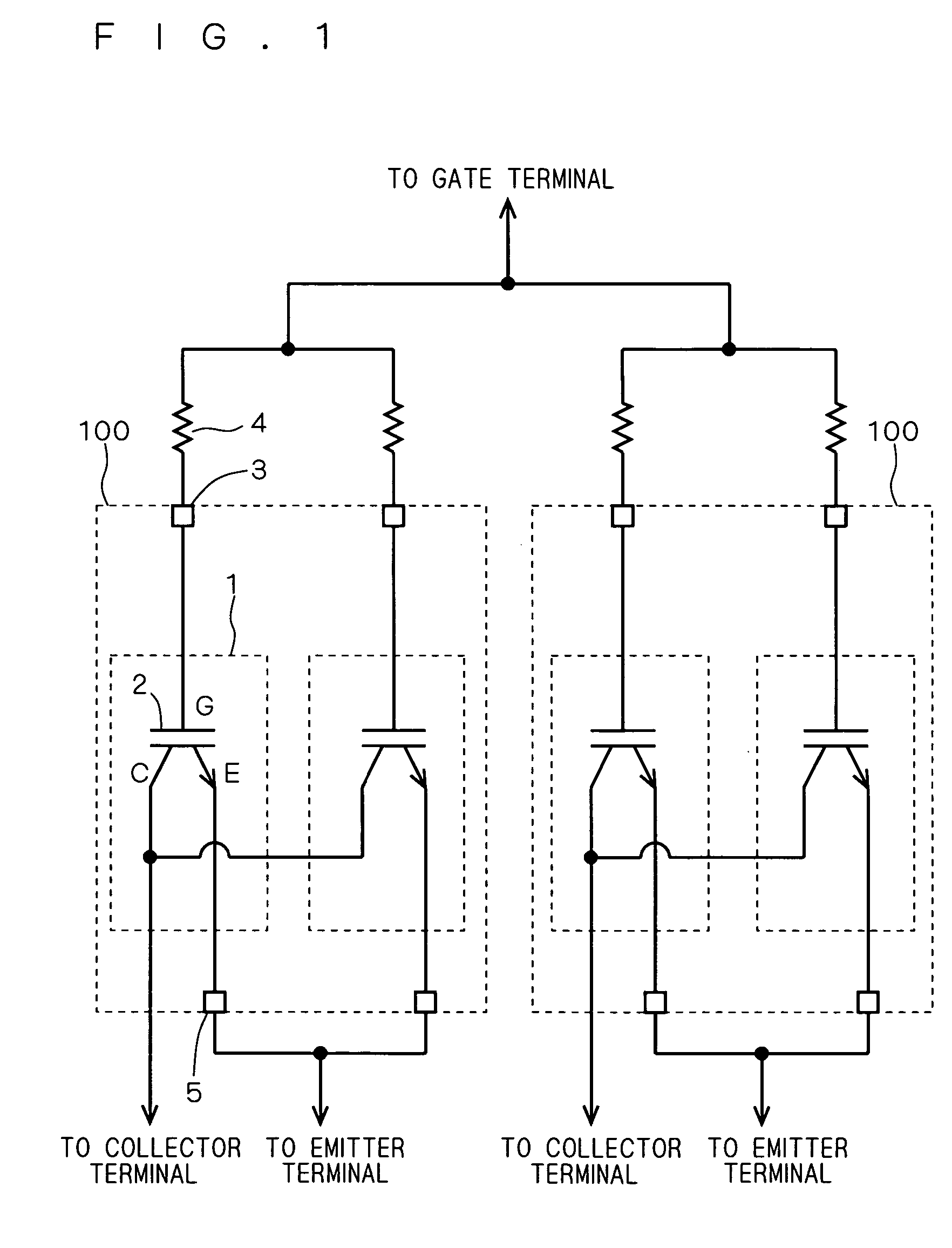
[0018]FIG. 1 is an equivalent circuit diagram of an IGBT module according to the present embodiment.

[0019] This IGBT module is configured with a plurality of IGBT chips (semiconductor chips) 100 (two IGBT chips 100 in FIG. 1) connected to each other. The IGBT chips 100 are each configured with a plurality of unit cells 1 (two unit cells 1 in FIG. 1) connected to each other.

[0020] The unit cells 1 each include one IGBT element 2. Gate voltage is applied to the gate G of the IGBT element 2 from a common gate terminal through a gate pad 3 and a gate resistor 4. Here, the gate G and gate pad 3 are connected to each other by an interconnect layer (not shown) within the IGBT chip 100. The gate pad 3 and gate resistor 4 are connected to each other by a bonding wire (not shown) provided outside the IGBT chip 100. That is, in FIG. 1, the resistor 4 has its first end connected to the gate pad 3 and its second end connected to the gate terminal.

[0021] Emitter voltage is applied to the emitt...

second preferred embodiment

[0029] In the IGBT module according to the first preferred embodiment, the gate resistor 4 is provided on the outer side with respect to the gate pad 3 (that is, outside the IGBT chip 100), however, the gate resistor 4 may be provided on the inner side with respect to the gate pad 3 (that is, within the IGBT chip 100).

[0030]FIG. 4 is an equivalent circuit diagram showing the configuration of an IGBT module according to a second preferred embodiment of the present invention. An IGBT chip 200 shown in FIG. 4 is configured by shifting the gate resistor 4 in the IGBT chip 100 shown in FIG. 1 from the outer side to the inner side with respect to the gate pad 3. For ease of illustration, FIG. 4 only shows one of a plurality of IGBT chips 200.

[0031] In FIG. 1, the gate resistor 4 is connected to the outer side with respect to the gate pad 3 by a bonding wire.

[0032] On the other hand, in FIG. 4, the gate resistor 4 is provided on the inner side with respect to the gate pad 3 (i.e., withi...

third preferred embodiment

[0041] In both the IGBT modules according to the first and second preferred embodiments, one gate pad 3 is provided for each gate resistor 4. In the IGBT module according to the second preferred embodiment, however, the gate resistor 4 is provided within the IGBT chip 200, and therefore, one gate pad 3 may be provided for each IGBT chip 200.

[0042]FIG. 6 is an equivalent circuit diagram showing the configuration of an IGBT module according to a third preferred embodiment. An IGBT chip 300 shown in FIG. 6 is configured by replacing the gate pads 3 in the IGBT chip 200 shown in FIG. 4 by a single gate pad 3. Specifically, in FIG. 6, the plurality of gate resistors 4 have their first ends connected to the gate G of a corresponding one of the IGBT elements 2 and their second ends connected to the gate pad 3 in common.

[0043] Therefore, the number of gate pads 3 can be reduced, which thus can reduce the IGBT chip 300 in area and can reduce the number of bonding wires connected to the gat...


PUM


Abstract

An IGBT module is configured with a plurality of IGBT cells connected to each other. The IGBT chips are each configured a plurality of unit cells connected to each other. The unit cells each include one IGBT element. Gate voltage is applied to the gate of the IGBT element from a common gate terminal through a gate pad and a gate resistor. Emitter voltage is applied to the emitter of the IGBT element from a common emitter terminal through an emitter pad. Collector voltage is applied to the collector of the IGBT element from a common collector terminal. The gate pad, gate transistor and emitter pad are provided for each of the unit cells. Thus obtained is an IGBT module capable of suppressing gate voltage oscillation without significantly increasing switching loss.

Description

BACKGROUND OF THE INVENTION [0001] 1. Field of the Invention [0002] The present invention relates to an IGBT (insulated gate bipolar transistor) module, and more particularly, to a technique for suppressing gate voltage oscillation in IGBT chips. [0003] 2. Description of the Background Art [0004] Gate insulated semiconductor devices such as IGBTs and MOSFETs have been used as power converters. An IGBT is equipped with both the high-speed operating characteristic offered by a MOSFET and the low on-state voltage characteristic offered by a bipolar transistor, and therefore, it has been widely used as a power converter such as an inverter. Further, IGBT chips having a rated current (an average current a chip can pass therethrough) of approximately several hundreds amperes have been offered recently, which contribute to size reduction of power modules. Generally, the rated current of an IGBT chip is proportional to its chip area. [0005] IGBTs have been dramatically improved in performan...

Claims


Application Information

Patent Timeline
Patent Type & Authority Applications(United States)
IPC IPC(8): H01L21/822H01L25/18H01L21/8234H01L23/538H01L23/58H01L25/00H01L25/04H01L25/07H01L27/02H01L27/04H01L27/06H01L27/082H01L27/088H01L29/73H01L29/739H01L29/78
CPCH01L27/0288H01L29/7395H01L2924/13055H01L2924/13091H01L2224/02166H01L24/05H01L2924/1305H01L2224/05553H01L2924/00H01L29/739H01L29/73
Inventor MOCHIZUKI, KOUICHITOMOMATSU, YOSHIFUMI
Owner MITSUBISHI ELECTRIC CORP
Why Eureka
Try Eureka