Recess type MOS transistor and method of manufacturing same

a mos transistor and mos technology, applied in the field of mos transistors, can solve the problems of hot carrier effect, hot carrier effect, gate control function to be lost in mos transistors, etc., and achieve the effect of preventing or substantially reducing the short channel effect, and improving the refresh characteristic of cell capacitors

Active Publication Date: 2005-09-08
SAMSUNG ELECTRONICS CO LTD
View PDF5 Cites 39 Cited by
  • Summary
  • Abstract
  • Description
  • Claims
  • Application Information

AI Technical Summary

Benefits of technology

[0035] Some embodiments of the invention provide a method of manufacturing a recess type MOS (Metal-Oxide Semiconductor) transistor, through which a threshold voltage characteristic of transistor may be improved and a junction leakage current may be reduced, improving the refresh characteristic of a cell capacitor. In the method, a short channel effect may be prevented or substantially reduced without reducing a density of a P-type or a N-type impurity that is ion-implanted in a third impurity region and in a channel impurity region when an open critical dimension and depth of a second trench are reduced.

Problems solved by technology

This causes a short channel effect that may cause a gate control function to be lost in a MOS transistor.
However, when a high electric field is applied in such a semiconductor device, a hot carrier effect may occur.
In the meantime, a continuous requirement for a high integration of semiconductor device makes the channel length be shorter, thus the transistor of the LDD structure also has a limitation in reducing the short channel effect and the hot carrier effect.
Furthermore, there is caused a punchthrough effect when the source and drain impurities diffuse toward side faces during operation of the transistor.
However, the method described above exhibits the following problems.

Method used


Image

  • Recess type MOS transistor and method of manufacturing same
  • Recess type MOS transistor and method of manufacturing same
  • Recess type MOS transistor and method of manufacturing same

Examples


Embodiment Construction

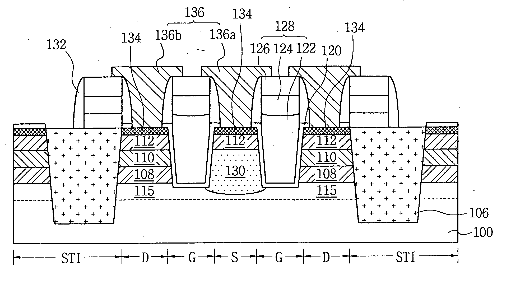
[0040] Exemplary embodiments of the invention are more fully described in detail with reference to FIGS. 2 and 3. The invention may be embodied in many different forms and should not be construed as being limited to the exemplary embodiments set forth herein. Rather, these exemplary embodiments are provided so that this disclosure is thorough and complete, and to convey the concept of the invention to those skilled in the art. For example, though it is described that a source region is connected to a bit line and a drain region is connected to a cell capacitor in a recess type MOS transistor, its opposite connection configuration may be provided. Furthermore, a recess and a trench may be used together with the same or similar meaning.

[0041]FIG. 3 is a cross-sectional diagram illustrating a structure of a recess type MOS transistor according to some embodiments of the invention.

[0042] Referring first to FIG. 3, a gate stack 128 is formed along an upper part of a gate insulation lay...


PUM


Abstract

The method of manufacturing a recess type MOS transistor improves a refresh characteristic. In the method, a channel impurity region is formed by ion implanting a first conductive impurity in an active region of a semiconductor substrate. Thereon, a second conductive impurity and the first conductive impurity are ion-implanted each alternately into the active region, to thus sequentially form first to third impurity regions having a dual diode structure on the channel impurity region, the second conductive impurity having conductivity opposite to the first conductive impurity. A trench is formed, and a gate insulation layer is formed in a gate region to produce a gate stack. The first conductive impurity is selectively ion-implanted in a source region, to thus form a fourth impurity region. A spacer is then formed in a sidewall of the gate stack, and the second conductive impurity is ion-implanted in the source/drain regions, to form a fifth impurity region.

Description

CROSS REFERENCE TO RELATED APPLICATIONS [0001] This application claims priority from Korean Patent Application No. 2003-95141, filed on Dec. 23, 2003, the content of which is hereby incorporated by reference in its entirety for all purposes. BACKGROUND OF THE INVENTION [0002] 1. Field of the Invention [0003] This disclosure relates to a semiconductor memory device, and more particularly, to a method of manufacturing a recess type MOS transistor, from which a refresh characteristic can be improved through an impurity region having a dual diode structure. [0004] 2. Description of the Related Art [0005] MOS (Metal-Oxide Semiconductor) devices are increasingly miniaturized in response to the desire to increase the integration of semiconductor devices. Channel lengths are reduced to the deep sub-micron level in order to increase an operating speed and current drive capability of the device. [0006] According to the gradual reduction of channel length, source and drain depletion regions ma...

Claims


Application Information

Patent Timeline
Patent Type & Authority Applications(United States)
IPC IPC(8): H01L21/336H01L21/8238
CPCH01L21/823412H01L21/823437H01L29/66659H01L27/0727H01L29/66621H01L21/823481H01L21/18
Inventor SEO, HYEOUNG-WONSONG, DU-HEONWON, DAE-JOONGLEE, SANG-HYUN
Owner SAMSUNG ELECTRONICS CO LTD
Why Eureka
Try Eureka