Method of depositing an amorphous carbon film for etch hardmask application

a technology of amorphous carbon film and etch hardmask, which is applied in the field of manufacturing integrated circuits, can solve the problems of low k material brittleness, and difficulty in producing features with little or no surface defects or feature deformation

Inactive Publication Date: 2005-09-15
APPLIED MATERIALS INC
View PDF73 Cites 80 Cited by
  • Summary
  • Abstract
  • Description
  • Claims
  • Application Information

AI Technical Summary

Benefits of technology

[0013] Aspects of the invention generally provide a method for depositing amorphous carbon materials. In one aspect, the invention provides a method for processing a substrate including positioning the substrate in a processing chamber, introducing a processing gas into the processing chamber, wherein the processing gas comprises one or more hydrocarbon compounds and an argon carrier gas, generating a plasma of the processing gas by applying power from a dual-frequency RF source, and depositing an amorphous carbon layer on the substrate.
[0014] In another aspect of the invention, a method is provided for processing a substrate including forming a dielectric material layer on a surface of the substrate, depositing one or more amorphous carbon layers on the dielectric material layer by a process comprising introducing a processing gas comprises one or more hydrocarbon compounds and an argon carrier gas, generating a plasma of the processing gas by applying power from a dual-frequency RF source, etching the one or more amorphous carbon layers to form a patterned amorphous carbon layer, and etching feature definitions in the dielectric material layer corresponding to the patterned one or more amorphous carbon layers.
[0015] In another aspect of the invention, a method is provided for processing a substrate including depositing one or more dielectric layers on a substrate surface, wherein at least one of the one or more dielectric layers comprise silicon, oxygen, and carbon and has a dielectric constant of about 3 or less, forming one or more amorphous carbon layers on the one or more dielectric layers by a process comprising introducing a processing gas comprises one or more hydrocarbon compounds and an argon carrier gas, generating a plasma of the processing gas by applying power from a dual-frequency RF source, defining a pattern in at least one region of the one or more amorphous carbon layers, forming feature definitions in the one or more dielectric layer by the pattern formed in the at least one region of the one or more amorphous carbon layers and depositing one or more conductive materials in the feature definitions.

Problems solved by technology

However, when low k material have been used in damascene formation, it has been difficult to produce features with little or no surface defects or feature deformation.
It has been observed that low k dielectric materials are often porous and susceptible to being scratched and damaged during removal of conductive materials, which results in defects being formed on the substrate surface.
Further, low k materials are often brittle and may deform under conventional polishing processes.
Such thinner resist materials (less than about 6000 Å) can be insufficient to mask underlying material layers during a pattern transfer step using a chemical etchant.
However, in some applications for forming semiconductor structures, it is difficult to remove hardmask materials from the substrate surface and the remaining hardmask material may detrimentally affect semiconductor processing.
Further, conventional hardmask materials may not provide sufficient etch selectivity between the material being etched and the hardmask to retain the desired dimensions of the features being formed.
Resist patterning problems are further compounded when lithographic imaging tools having deep ultraviolet (DUV) imaging wavelengths (e. g., less than about 250 nanometers (nm)) are used to generate the resist patterns.
Additionally, the increased reflective nature of many underlying materials, such as polysilicon, metals, and metal siuicides at such DUV wavelengths, can degrade the resulting resist patterns.
However, ARC materials, like hardmask materials are difficult to remove and may leave residues behind that potentially interfere with subsequent integrated circuit fabrication steps.

Method used


Image

  • Method of depositing an amorphous carbon film for etch hardmask application
  • Method of depositing an amorphous carbon film for etch hardmask application
  • Method of depositing an amorphous carbon film for etch hardmask application

Examples


examples

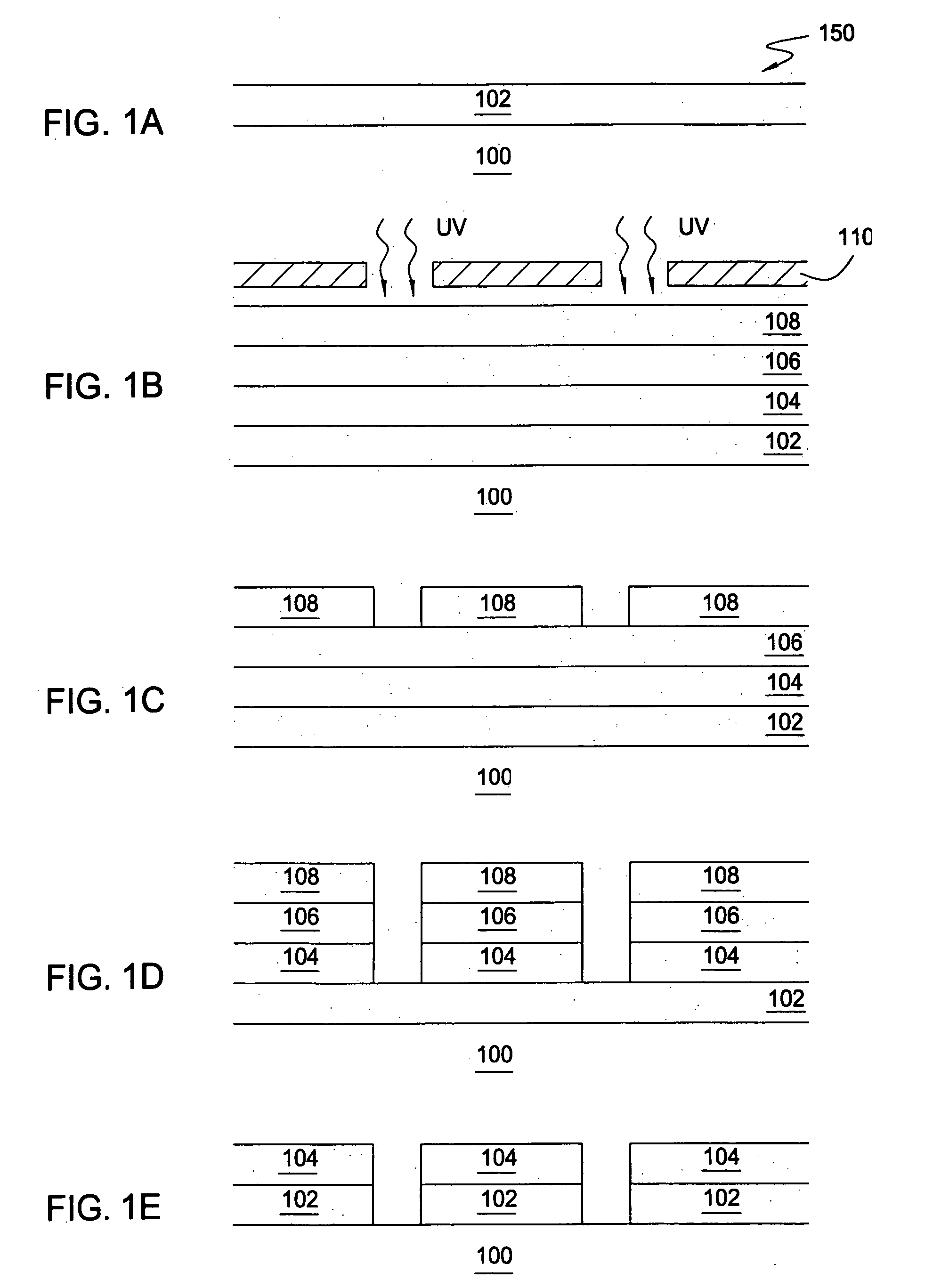
[0078] The following examples demonstrate various embodiments of the adhesion processes described herein as compared to a standard interlayer stack to illustrate the improved interlayer adhesion. The samples were undertaken using a chemical vapor deposition chamber, and in dual processing station Producer™ 200 mm and 300 mm processing chambers, which includes a solid-state dual frequency RF matching unit with a two-piece quartz process kit, both fabricated and sold by Applied Materials, Inc., Santa Clara, Calif.

[0079] Amorphous carbon films were deposited as follows. An amorphous carbon layer was deposited with a single frequency and helium carrier gas by introducing propylene, C3H6, at a flow rate of about 1000 sccm and helium at a flow rate of about 650 sccm, optionally maintaining the chamber at a substrate temperature of about 350° C., maintaining a chamber pressure of about 7 Torr, positioning a gas distributor at about 240 mils from the substrate surface, and applying a RF po...


PUM

PropertyMeasurementUnit
frequencyaaaaaaaaaa
dielectric constantaaaaaaaaaa
imaging wavelengthsaaaaaaaaaa

Abstract

Methods are provided for depositing amorphous carbon materials. In one aspect, the invention provides a method for processing a substrate including forming a dielectric material layer on a surface of the substrate, depositing an amorphous carbon layer on the dielectric material layer by introducing a processing gas comprises one or more hydrocarbon compounds and an argon carrier gas, and generating a plasma of the processing gas by applying power from a dual-frequency RF source, etching the amorphous carbon layer to form a patterned amorphous carbon layer, and etching feature definitions in the dielectric material layer corresponding to the patterned amorphous carbon layer. The amorphous carbon layer may act as an etch stop, an anti-reflective coating, or both.

Description

BACKGROUND OF THE DISCLOSURE [0001] 1. Field of the Invention [0002] The invention relates to the fabrication of integrated circuits and to a process for depositing materials on a substrate and the structures formed by the materials. [0003] 2. Description of the Related Art [0004] One of the primary steps in the fabrication of modern semiconductor devices is the formation of metal and dielectric layers on a substrate by chemical reaction of gases. Such deposition processes are referred to as chemical vapor deposition or CVD. Conventional thermal CVD processes supply reactive gases to the substrate surface where energy-induced chemical reactions take place to produce a desired layer. [0005] CVD processes are useful in forming vertical and horizontal interconnects by a damascene or dual damascene method involving the deposition and patterning of one or more material layers. In the damascene method, one or more dielectric materials, such as the low k dielectric materials (i.e., having ...

Claims


Application Information

Patent Timeline
Patent Type & Authority Applications(United States)
IPC IPC(8): H01L21/469
CPCH01L21/02115H01L21/02274H01L21/0276H01L21/31122H01L21/31144G03F7/094H01L21/7681H01L21/76829H01L21/7684G03F7/091H01L21/76802
Inventor WANG, YUXIANG MAYRATHI, SUDHA S.R.KWAN, MICHAEL CHIUM'SAAD, HICHEM
Owner APPLIED MATERIALS INC
Why Eureka
Try Eureka