Level conversion circuit and serial/parallel conversion circuit with level conversion function

a level conversion circuit and level conversion function technology, applied in logic circuit coupling/interface arrangement, pulse technique, instruments, etc., can solve the problems of insufficient high-speed operation, inferior crystal quality of low-temperature polysilicon tft, and inability to reduce the occupied area, etc., to achieve low power consumption and high speed

Inactive Publication Date: 2005-09-22
MITSUBISHI ELECTRIC CORP
View PDF3 Cites 23 Cited by
  • Summary
  • Abstract
  • Description
  • Claims
  • Application Information

AI Technical Summary

Benefits of technology

[0015] An object of the present invention is to provide a level conversion circuit capable of converting a signal of small voltage amplitude into a signal of large voltage amplitude at a high speed and with low power consumption as well as a serial / parallel level conversion circuit using the level conversion circuit.

Problems solved by technology

Thus, as compared with a MOS transistor using single-crystal silicon, the crystal quality of the low-temperature polysilicon TFT is inferior.
Therefore, the current drivability of the output drive transistor is small, and a level-converted signal of a large amplitude that is held in the second capacitance element cannot be discharged at a high speed, resulting in a problem that a high-speed operation is not ensured.
Accordingly, the input buffer circuit has a large number of transistor elements, resulting in a problem that the occupied area cannot be reduced.
In addition, if the transistor elements have greatly-varied threshold voltages, offset in a comparison stage of the current-mirror type input buffer circuit cannot be compensated for, resulting in a problem that an accurate input signal cannot be generated.
Accordingly, in the output drive stage, both of charging and discharging drive transistors are in an ON state, resulting in a problem that a through current flows all the time.
Accordingly, it is required to provide capacitance elements respectively for the high-side drive transistor and the low-side transistor on the node receiving the input signal, resulting in a problem that the load of the input signal increases.
Thus, if a skew occurs between the complementary input signals, the signal on the internal output node is coupled via the second drive transistor to the input signal, resulting in a problem that the internal output node cannot sufficiently charged and thus an accurately level-converted signal cannot be generated.

Method used


Image

  • Level conversion circuit and serial/parallel conversion circuit with level conversion function
  • Level conversion circuit and serial/parallel conversion circuit with level conversion function
  • Level conversion circuit and serial/parallel conversion circuit with level conversion function

Examples


first embodiment

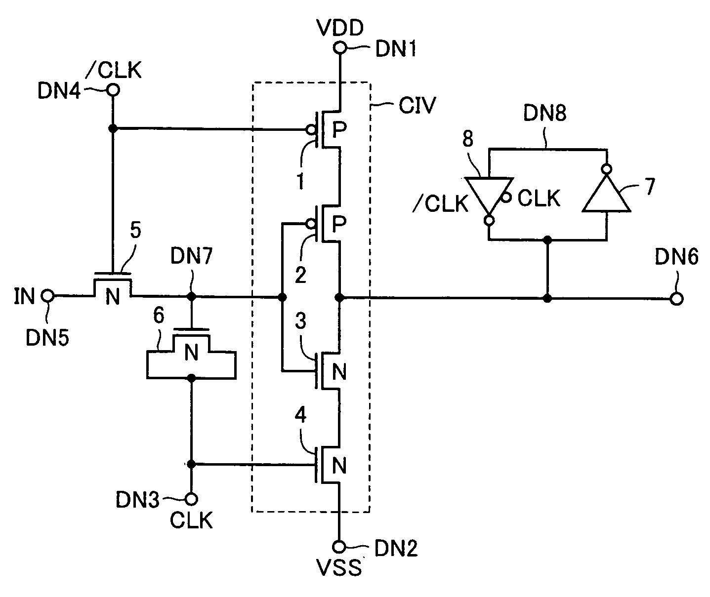
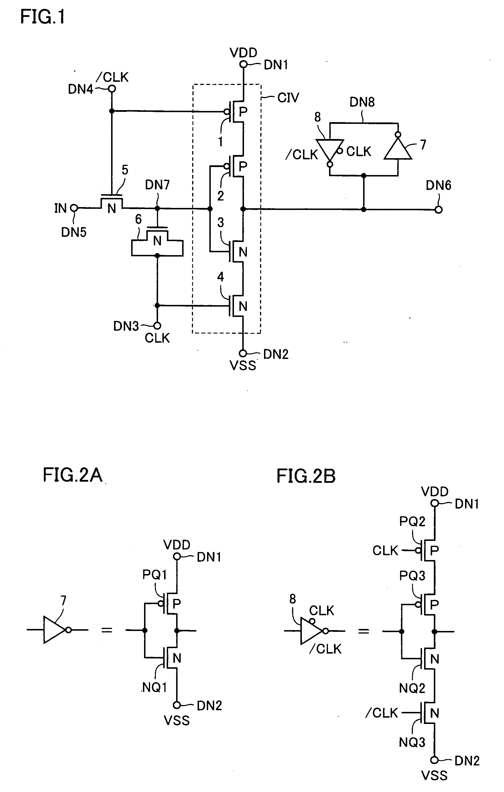
[0069]FIG. 1 shows a configuration of a level conversion circuit according to a first embodiment of the present invention. Referring to FIG. 1, the level conversion circuit includes an N-channel MOS transistor (insulated gate field effect transistor) 5 transmitting an input signal IN applied to an input node DN5 to an internal node DN7 according to a clock signal / CLK applied to an input node DN4, a MOS-type capacitance element (hereinafter referred to as MOS capacitor) 6 coupled to internal node DN7 and selectively forming a capacitor according to a clock signal CLK from a clock input node DN3, a clocked inverter CIV selectively activated according to clock signals CLK and / CLK and driving, when activated, an internal output node DN6 according to the signal on internal node DN7, and an inverter 7 and a clocked inverter 8 that constitute a latch circuit latching a signal voltage on internal output node DN6.

[0070] When this level conversion circuit is used in a display device (displ...

second embodiment

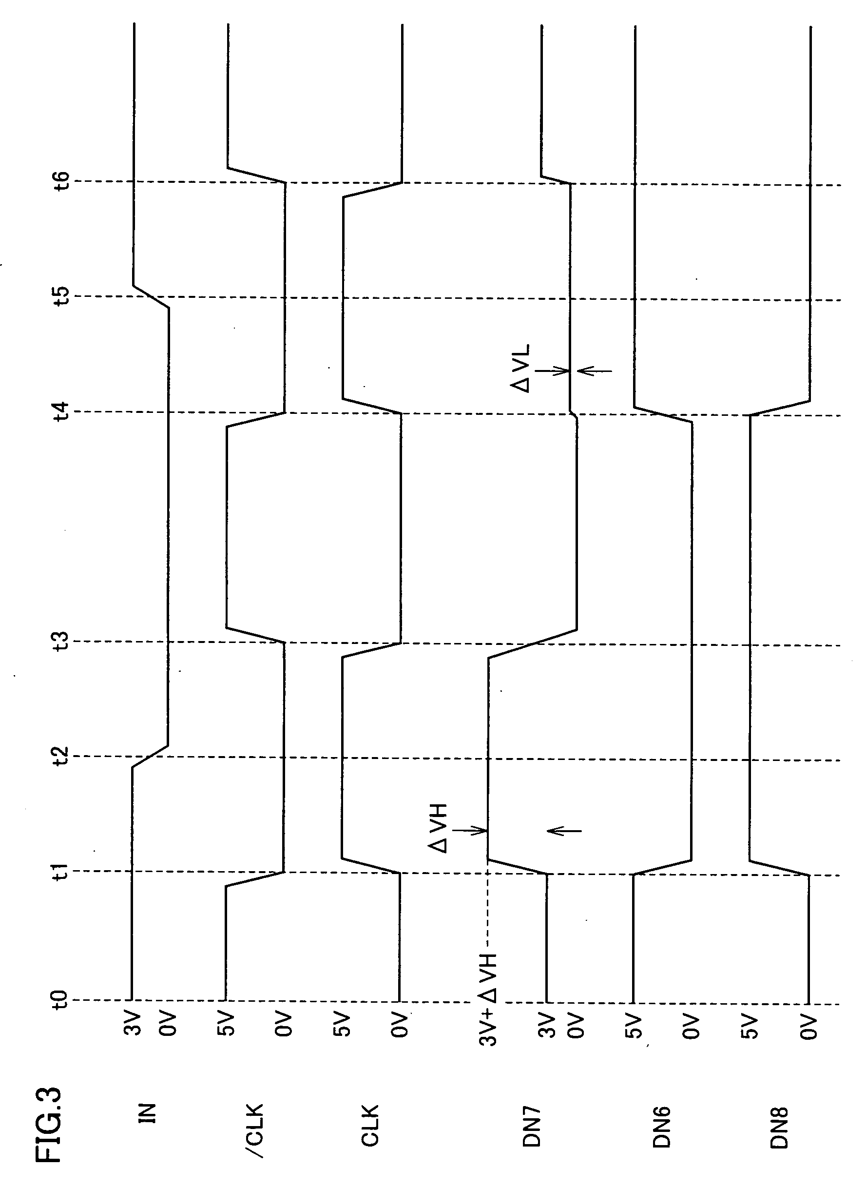
[0095]FIG. 4 shows a configuration of a level conversion circuit according to a second embodiment of the present invention. The configuration of the level conversion circuit shown in FIG. 4 differs from that of the level conversion circuit shown in FIG. 1 in that, to low-side power supply node DN2 of clocked inverter CIV, clock signal / CLK is applied instead of the measurement reference voltage (ground voltage VSS). Other configuration of the level conversion circuit shown in FIG. 4 is identical to that of the level conversion circuit shown in FIG. 1. Therefore, like components are denoted by like reference numerals and the detailed description thereof is not repeated.

[0096] In the level conversion circuit shown in FIG. 4, clock signal CLK changes with a delay to clock signal / CLK.

[0097]FIG. 5 is a signal waveform diagram representing an operation of the level conversion circuit shown in FIG. 4 in the case where the clock skew large. As shown in FIG. 5, it is assumed now that inpu...

third embodiment

[0115]FIG. 8 shows a configuration of a level conversion circuit according to a third embodiment of the present invention. The configuration of the level conversion circuit shown in FIG. 8 differs from that of the level conversion circuit shown in FIG. 1 or 4 in that, the gate of P-channel MOS transistor 1 of clocked inverter CIV that is connected to high-side power supply node DN1 is connected to internal node DN7 and clock signal / CLK is applied to the gate of P-channel MOS transistor 2 connected to internal output node DN6. Similarly, clock signal CLK is applied to the gate of N-channel MOS transistor 3 and the gate of N-channel MOS transistor 4 connected to low-side power supply node DN2 is connected to internal node DN7. Further, to low-side power-supply node DN2, reference voltage VSS or clock signal / CLK is applied. Other configuration of the level conversion circuit shown in FIG. 8 is identical to the level conversion circuit shown in FIG. 1 or 4. Therefore, like components ...


PUM


Abstract

A MOS capacitor receiving a clock signal complementary to a sampling clock signal is provided at an input of a clocked inverter that is activated after sampling an input signal to perform level conversion. A charge pump operation of the MOS capacitor is performed in parallel with the activation of the clocked inverter. The power consumption of and the area occupied by a level conversion circuit converting a voltage amplitude of the input signal are reduced without deteriorating a high-speed operating characteristics.

Description

BACKGROUND OF THE INVENTION [0001] 1. Field of the Invention [0002] The present invention relates to a level conversion circuit using insulated gate field effect transistors (MOS transistors). In particular, the present invention relates to a level shift circuit having a latch function and used for display devices formed using, for example, liquid-crystal elements or organic electroluminescence (EL) elements. More specifically, the present invention relates to a circuit configuration for latching and level-shifting a pixel data signal applied to a display pixel. [0003] 2. Description of the Background Art [0004] In a display device using liquid-crystal elements or organic EL (electroluminescence) elements as display pixel elements, a level conversion circuit is employed for enlarging a signal amplitude. For example, in order to accurately drive the display pixel elements in accordance with a display signal, for achieving gradational display, the amplitude of an image data signal is ...

Claims


Application Information

Patent Timeline
Patent Type & Authority Applications(United States)
IPC IPC(8): G09G3/20H03K19/0185G11C19/18G11C27/02H03L7/06H03M9/00
CPCG09G3/20G09G2310/027H03M9/00G09G2310/0294H03K19/01855G09G2310/0289H05B3/20H05B3/10H05B2203/016H05B2203/019H05B2203/02H05B2203/021
Inventor TOBITA, YOUICHI
Owner MITSUBISHI ELECTRIC CORP
Why Eureka
Try Eureka