Self-aligned split-gate NAND flash memory and fabrication process

a technology of nand flash memory and self-aligning, which is applied in the direction of digital storage, semiconductor devices, instruments, etc., can solve the problems of difficult to form a high-voltage coupling ratio which is sufficient for program and erase operations, and is used in very high-density data storage applications. achieve the effect of enhancing high-voltage coupling and reducing channel resistan

Active Publication Date: 2005-09-22
SILICON STORAGE TECHNOLOGY
View PDF5 Cites 30 Cited by
  • Summary
  • Abstract
  • Description
  • Claims
  • Application Information

AI Technical Summary

Benefits of technology

[0013] These and other objects are achieved in accordance with the invention by providing a self-aligned split-gate NAND flash memory cell array and process of fabrication in which rows of self-aligned split-gate cells are formed between a bit line diffusion and a common source diffusion in the active area of a substrate. Each cell has control and floating gates which are stacked and self-aligned with each other, and erase and select gates which are split from and self-aligned with the stacked gates, with select gates at both ends of each row which partially overlap the bit line the source diffusions. The channel regions beneath the erase gates are heavily doped to reduce the resistance of the channel between the bit line and source diffusions, and the floating gates are surrounded by the other gates in a manner which provides significantly enhanced high voltage coupling to the floating gates from the other gates. The array is biased so that all of the memory cells in it can be erased simultaneously, while programming is bit selectable.

Problems solved by technology

The relatively size of such cells prevents them from being used in very high density data storage applications.
However, as fabrication processes advance toward smaller geometries, e.g. tens of nanometers, it is difficult to form a high-voltage coupling ratio which is sufficient for program and erase operations while maintaining a small cell size and meeting stringent reliability requirements such as 10-year data retention and 1,000,000 cycling operations between failures.

Method used


Image

  • Self-aligned split-gate NAND flash memory and fabrication process
  • Self-aligned split-gate NAND flash memory and fabrication process
  • Self-aligned split-gate NAND flash memory and fabrication process

Examples


Embodiment Construction

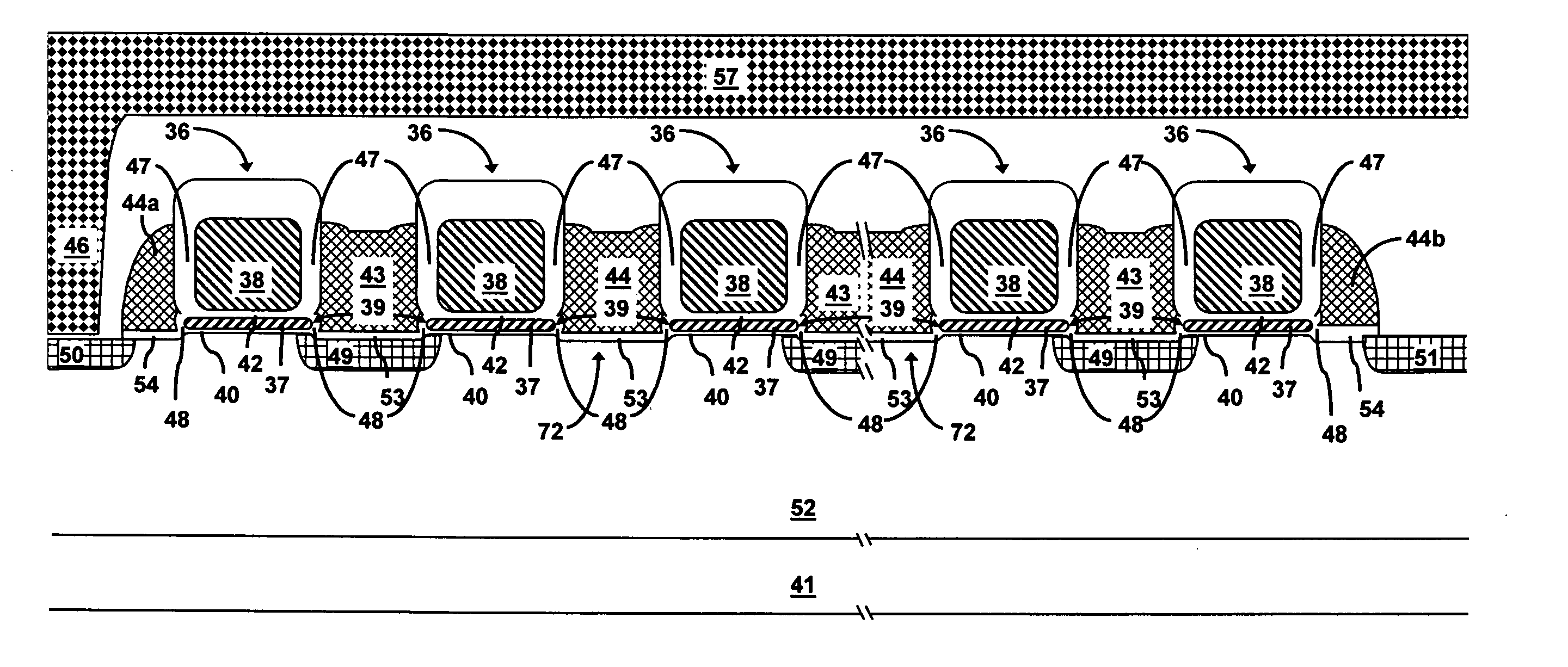
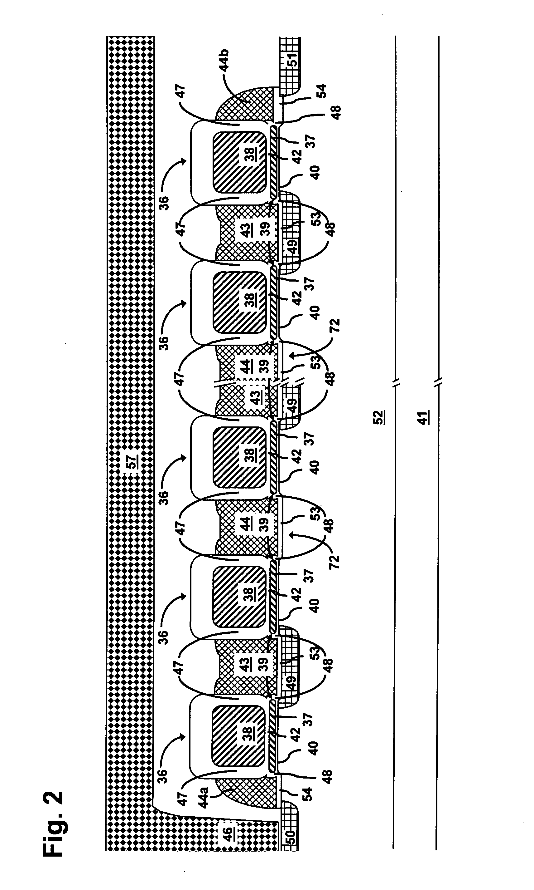
[0023] As illustrated in FIGS. 2 and 3, the memory includes an array of split-gate NAND flash memory cells 36, each of which has a floating gate 37 and a control gate 38, with the control gate being positioned above and in vertical alignment with the floating gate.

[0024] The floating gates are relatively thin and are fabricated of a conductive material such as polysilicon or amorphous silicon, with a preferred thickness on the order of 100 Å to 1000 Å. Thin gate insulators 40, typically a thermal oxide, are positioned between the floating gates and the underlying the substrate.

[0025] The control gates are narrower in horizontal dimension and thicker in vertical dimension than the floating gates, with the edge portions of the floating gates extending laterally beyond the edge portions of the control gates. The control gates are fabricated of a conductive material such as a doped polysilicon or polycide, and each of the control gates is insulated from the floating gate beneath it by...


PUM


Abstract

Self-aligned split-gate NAND flash memory cell array and process of fabrication in which rows of self-aligned split-gate cells are formed between a bit line diffusion and a common source diffusion in the active area of a substrate. Each cell has control and floating gates which are stacked and self-aligned with each other, and erase and select gates which are split from and self-aligned with the stacked gates, with select gates at both ends of each row which partially overlap the bit line the source diffusions. The channel regions beneath the erase gates are heavily doped to reduce the resistance of the channel between the bit line and source diffusions, and the floating gates are surrounded by the other gates in a manner which provides significantly enhanced high voltage coupling to the floating gates from the other gates. The memory cells are substantially smaller than prior art cells, and the array is biased so that all of the memory cells in it can be erased simultaneously, while programming is bit selectable.

Description

BACKGROUND OF THE INVENTION [0001] 1. Field of Invention [0002] This invention pertains generally to semiconductor memory devices and, more particularly, to a self-aligned split-gate NAND flash memory and process of fabricating the same. [0003] 2. Related Art [0004] Nonvolatile memory is currently available in several forms, including electrically programmable read only memory (EPROM), electrically erasable programmable read only memory (EEPROM), and flash EEPROM. Flash memory has been widely used for high volume data storage in devices such as memory cards, personal digital assistants (PDA's), cellular phones, and MP3 players. Such applications require high density memory, with smaller cell size and reduced cost of manufacture. [0005] NOR-type stack-gate flash memory cells typically have a bit line contact, a source region, a floating gate, and a control gate, with the control gate being positioned directly above the floating gate. The relatively size of such cells prevents them fr...

Claims


Application Information

Patent Timeline
Patent Type & Authority Applications(United States)
IPC IPC(8): G11C16/00G11C16/04H01L21/8247H01L27/105H01L27/115
CPCG11C16/0483G11C2216/04H01L27/11524H01L27/11521H01L27/115H10B41/35H10B69/00H10B41/30
Inventor CHEN, CHIOU-FENGCHO, CALEB YU-SHENGCHEN, MING-JERFAN, DER-TSYRTUNTASOOD, PRATEEP
Owner SILICON STORAGE TECHNOLOGY
Why Eureka
Try Eureka