Hardenable pressure-sensitive adhesive sheet for semiconductor and process for producing semiconductor device

a technology of pressure-sensitive adhesives and semiconductors, applied in the direction of heat-activated film/foil adhesives, film/foil adhesives, transportation and packaging, etc., can solve the problems of warpage between substrates and chips, difference in thermal expansion coefficient between silicon chips, and stress on the hpsa layer interposed between silicon chips and substrates, etc., to achieve excellent versatility and adherence, and high reliability

Inactive Publication Date: 2005-09-22
LINTEC CORP
View PDF7 Cites 28 Cited by
  • Summary
  • Abstract
  • Description
  • Claims
  • Application Information

AI Technical Summary

Benefits of technology

[0023] By virtue of the present invention, there is provided a HPSA sheet for semiconductor excellent in versatility and adherence, by which a semiconductor device of high reliability free from the warpage and delamination of substrate and chips even exposed under heat cycle conditions can be produced.

Problems solved by technology

However, in the IR reflow operation, etc. of reliability test, the occurrence of warpage of substrate and chips and delamination between substrate and chips has tended to increase in accordance with a decrease of the thickness of silicon chips.
The cause of this problem would be a difference in thermal expansion coefficient between silicon chips and surface material (organic material such as a polyimide) of substrate on which the silicon chips are mounted.
Consequently, under heat cycle conditions, the HPSA layer interposed between the silicon chips and the substrate suffers a stress attributed to the difference in thermal expansion coefficient.
In particular, when the storage modulus of the HPSA layer is high, warpages of the substrate and chips and delamination between the substrate and chips have been happened.

Method used


Image

  • Hardenable pressure-sensitive adhesive sheet for semiconductor and process for producing semiconductor device

Examples


example

[0086] The present invention will be further illustrated below with reference to the following Examples, which however in no way limit the scope of the invention.

[Preparation of HPSA Sheet for Semiconductor]

[0087] Base material: A polyethylene film (100 μm thickness and 32 mN / m surface tension) was used.

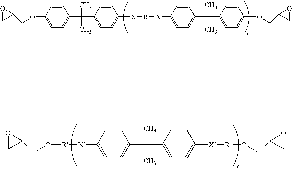
[0088] HPSA: The compositions are listed in Table 1. HPSA sheets for semiconductor were obtained by coating the base material with each of the listed HPSA compositions and drying the coated material so that the coating thickness was 20 μm.

[0089] The storage modulus and glass transition temperature (temperature at which tan δ was maximized) of HPSA layers after thermal curing were measured in the following manner. The base material was coated with each of the HPSAs and dried so that the coating thickness was 200 μm. Then, the base material was peeled off (when a radiation curable component was contained, the delamination was carried out after exposure to radiation rays). Thermal c...


PUM

PropertyMeasurementUnit
storage modulusaaaaaaaaaa
Tgaaaaaaaaaa

Abstract

Disclosed herein is a hardenable pressure-sensitive adhesive sheet enabling production of a semiconductor device of high reliability while preventing the occurrence of package cracking and other failure; and a process for producing a semiconductor device with the use of the hardenable pressure-sensitive adhesive sheet. There is provided a hardenable pressure-sensitive adhesive sheet having a hardenable pressure-sensitive adhesive layer comprising a pressure-sensitive component (A) and an epoxy resin (B), wherein the hardenable pressure-sensitive adhesive layer after thermal curing has a storage modulus of 1.0×10⁷ Pa or below at 100° C. and 1.0×10⁵ Pa or above at 160° C.

Description

FIELD OF THE INVENTION [0001] The present invention relates to a novel hardenable pressure-sensitive adhesive (hereinafter “HPSA”, and “pressure-sensitive adhesive” is called “PSA”) sheet for semiconductor and process for producing a semiconductor device. More particularly, the present invention relates to a HPSA sheet suitable for use in the steps of dicing a silicon wafer, etc. and effecting die bonding thereof to a lead frame, and relates to a process for producing a semiconductor device with the use of the HPSA sheet. BACKGROUND OF THE INVENTION [0002] A semiconductor wafer of silicon, gallium arsenide, etc. is produced in large diameter. The wafer is sequentially subjected to the steps of cut separation (dicing) into small element pieces (IC chips) and mounting thereof. In particular, a semiconductor wafer in the state of being stuck to a PSA sheet is sequentially subjected to the steps of dicing, washing, drying, expanding and pick-up and thereafter to the subsequent step of b...

Claims


Application Information

Patent Timeline
Patent Type & Authority Applications(United States)
IPC IPC(8): C09J4/02C09J7/22C09J7/35C09J7/38C09J133/00C09J163/00H01L21/00H01L21/52H01L21/68
CPCC09J7/0242C09J7/0246C09J2203/326C09J2463/00Y10T156/1062H01L21/6836H01L2221/68327Y10T156/11Y10T428/28H01L21/67132C09J7/35C09J7/38C09J7/22H01L21/78
Inventor SAIKI, NAOYAYAMAZAKI, OSAMUHAMASAKI, AKIE
Owner LINTEC CORP
Why Eureka
Try Eureka