Thin-film transistor formed on insulating substrate

a thin-film transistor and substrate technology, applied in the direction of transistors, semiconductor devices, electrical devices, etc., can solve the problems of non-uniform device characteristics, reduced non-uniform probability of grain boundary presence, etc., to achieve reduced possibility of device destruction, high-speed operation, and reduced non-uniform device characteristics

Inactive Publication Date: 2005-09-29
ADVANCED LCD TECH DEVMENT CENT
View PDF10 Cites 25 Cited by
  • Summary
  • Abstract
  • Description
  • Claims
  • Application Information

AI Technical Summary

Benefits of technology

[0015] With this structure, the probability is substantially zero that crystal grain boundaries, which extend in parallel to the inner and outer peripheries of the ring-shaped gate, are present in the channel region. Thus, there is substantially no grain boundary that hinders flow of electrons between the source and drain, and the high-speed operation is enabled. In addition, the non-uniformity in characteristics of devices, which results from non-uniformity in probability of presence of

Problems solved by technology

In addition, the non-uniformity in characteristics of devices, which results f

Method used


Image

  • Thin-film transistor formed on insulating substrate
  • Thin-film transistor formed on insulating substrate
  • Thin-film transistor formed on insulating substrate

Examples


first embodiment

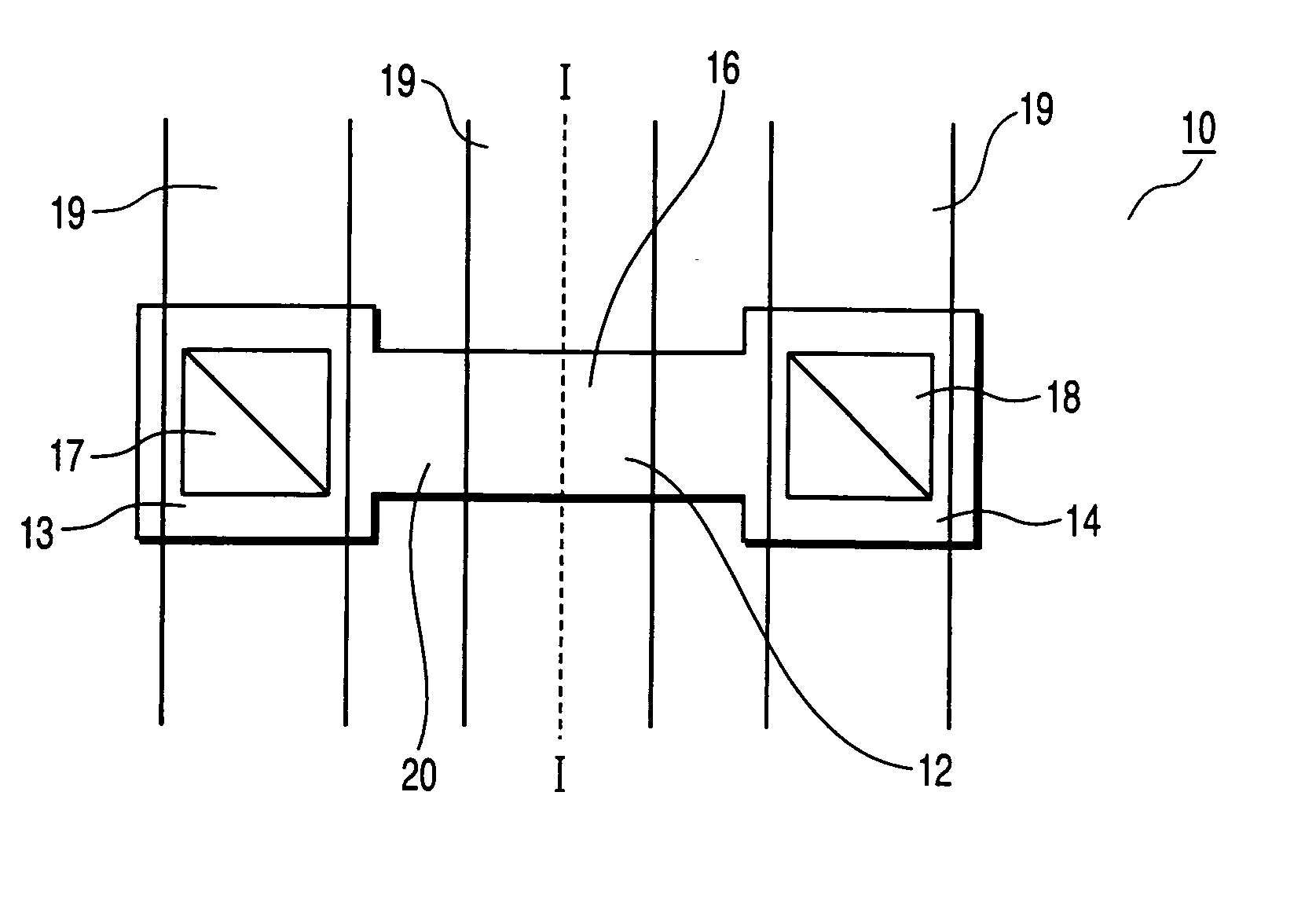
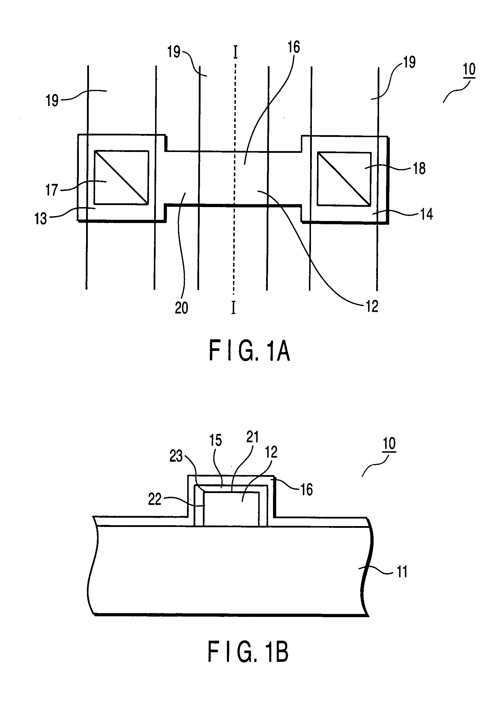
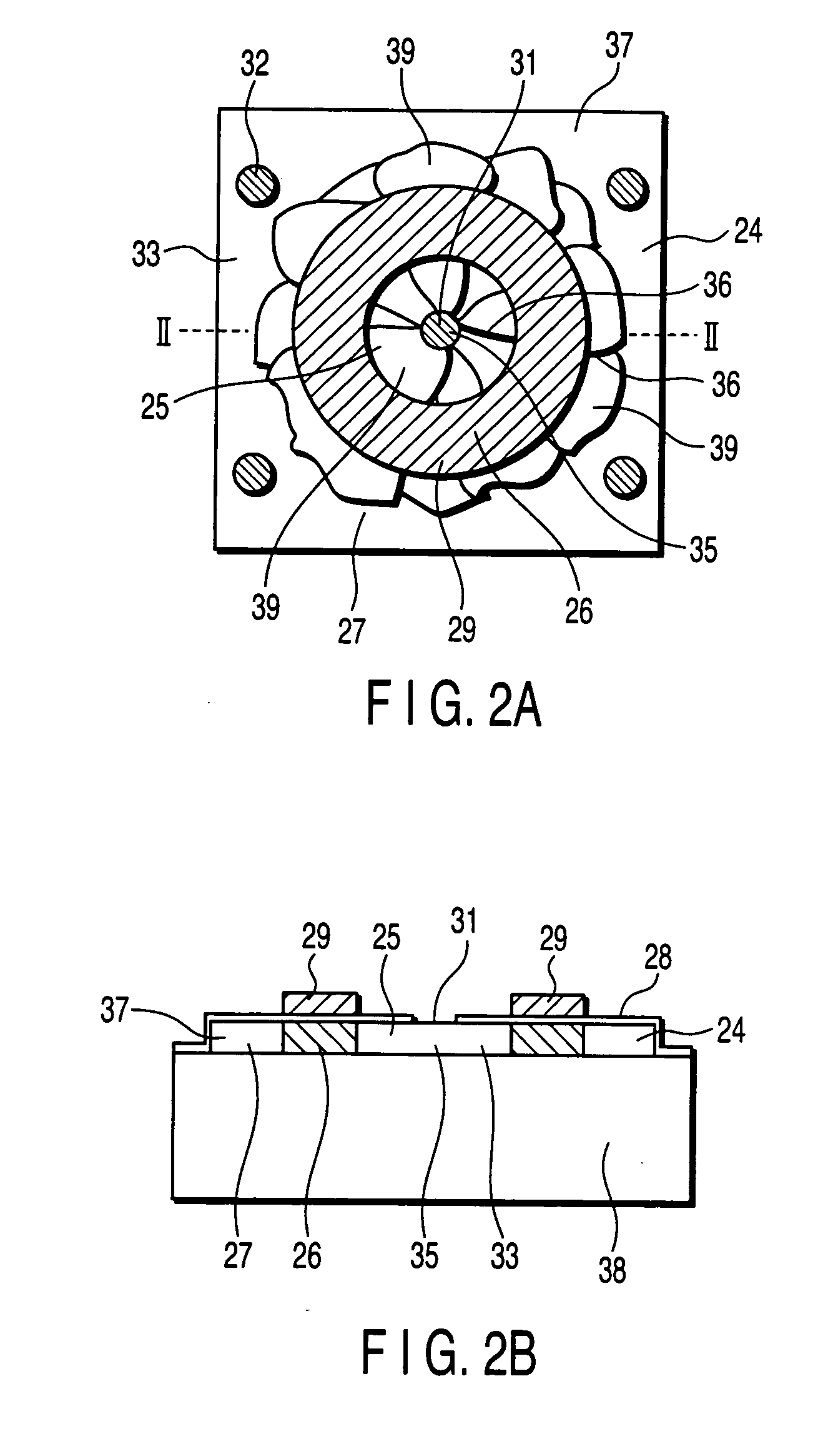
[0051]FIG. 2A and FIG. 2B show an example of the structure of a thin-film transistor according to a first embodiment of the present invention. FIG. 2A is a plan view and FIG. 2B is a cross-sectional view taken along line II-II in FIG. 2A.

[0052] As is shown in FIG. 2A and FIG. 2B, the thin-film transistor according to the first embodiment of the invention is formed on a semiconductor island 33 that is formed of a thin-film semiconductor 24 with a thickness of, e.g. 100 nm thick on an insulating substrate 38. A glass substrate, for instance, is used as the insulating substrate 38. In particular, it is preferable that a no-alkali glass substrate be used as the insulating substrate 38. It is also possible to use a quartz substrate or a plastic substrate, depending on necessity. For electrical isolation between neighboring devices, each thin-film semiconductor 24 is formed as a square thin-film semiconductor island 33 with a dimension of, e.g. 15 μm on each side. The shape of the semico...

second embodiment

[0079]FIG. 9A is a plan view that shows the structure of a second embodiment of the invention, and FIG. 9B is a cross-sectional view taken along line IX-IX in FIG. 9A. Like the structure shown in FIG. 2A, a semiconductor island 69 on an insulating substrate 71 is provided with a source region 61, a channel region 62, a drain region 63, a gate insulation film 64, a gate electrode 65, a source contact hole 66 and drain contact holes 68.

[0080] In the thin-film transistor shown in FIG. 2A, the channel region is doped with phosphorus (in the case of a PMOS transistor) or boron (in the case of an NMOS transistor) with a concentration of 1016 / cm3 to 1017 / cm3. In the second embodiment, an offset region 70, which has the same impurity concentration as the channel region, is provided between the drain region 63 and the channel region 62. The presence of the offset region 70 facilitates extension of a depletion layer in this region, and thus an increase in electric field at the end of the dra...

third embodiment

[0081]FIG. 10A is a plan view that shows the structure of a third embodiment of the invention, and FIG. 10B is a cross-sectional view taken along line X-X in FIG. 10A.

[0082] Like the structure shown in FIG. 9A, a semiconductor island 69 on an insulating substrate 71 is provided with a source region 61, a channel region 62, a drain region 63, a gate insulation film 64, a gate electrode 65, a source contact hole 66 and drain contact holes 68.

[0083] The thin-film transistor shown in FIG. 10A differs from the thin-film transistor shown in FIG. 2A in that an LDD (lightly doped drain) region 73 is provided between the drain region 63 and the channel region 62. The LDD region 73 is doped with impurities with a concentration that is lower than the concentration in the drain region 63 and is higher than the concentration in the channel region 62. The LDD region 73 is doped with the same kind of impurities as in the drain region with a concentration of 1018 / cm3. The presence of the LDD regi...


PUM


Abstract

There is provided a thin-film transistor that is formed on an insulating substrate, is capable of a high-speed operation, has small non-uniformity among devices, is hardly susceptible to device destruction due to high voltage, and is free from the effect of a parasitic transistor that forms at an edge part of an Si island. The thin-film semiconductor device is formed using a thin-film semiconductor provided on the insulating substrate and includes a gate region for formation of a channel region through which a drain current flows. The gate region has a ring shape in plan on the insulating substrate. High concentration impurity-doped regions are dividedly provided on an inside and an outside of the ring-shaped gate region, and the channel region is formed of a plurality of fan-shaped semiconductor single-crystal portions.

Description

CROSS-REFERENCE TO RELATED APPLICATIONS [0001] This application is based upon and claims the benefit of priority from prior Japanese Patent Application No. 2004-085542, filed Mar. 23, 2004, the entire contents of which are incorporated herein by reference. BACKGROUND OF THE INVENTION [0002] 1. Field of the Invention [0003] The present invention relates to a thin-film semiconductor device that is formed on a substrate with an insulating surface such as a glass substrate. In particular, the invention relates to a thin-film transistor with a high breakdown voltage, which is formed using a crystallized thin-film semiconductor formed on the substrate. [0004] 2. Description of the Related Art [0005] In order to drive an active-matrix flat-panel display that is employed as a display for image information or text information, attention has been paid to the use of thin-film transistors (TFTs) that are formed on an insulating substrate. In addition, the thin-film transistors have been put to ...

Claims


Application Information

Patent Timeline
IPC IPC(8): H01L21/336H01L21/77H01L21/8236H01L21/84H01L27/12H01L29/04H01L29/786
CPCH01L27/1285H01L27/1296H01L29/78696H01L29/66757H01L29/04
Inventor NAKANO, FUMIKIKAWACHI, GENSHIRONAKAZAKI, YOSHIAKITSUBOI, SHINZOENDO, TAKAHIKOKATO, TOMOYA
Owner ADVANCED LCD TECH DEVMENT CENT
Why Eureka
Try Eureka