Chamber cleaning method

a cleaning method and chamber technology, applied in the direction of cleaning using liquids, coatings, chemistry apparatus and processes, etc., can solve the problems of less stable amorphous silicon than polysilicon affecting device performance and reliability, and affecting the stability of amorphous silicon in single-wafer processing applications

Inactive Publication Date: 2005-09-29
TAIWAN SEMICON MFG CO LTD
View PDF10 Cites 23 Cited by
  • Summary
  • Abstract
  • Description
  • Claims
  • Application Information

AI Technical Summary

Problems solved by technology

Accordingly, device performance and reliability can be adversely affected by such factors as interfacial defects, defect precursors and diffusion of dopants through gate dielectrics, as well as unintended variations in thickness in the gate oxide layer among central and peripheral regions of the layer.
However, it has been found that in spite of the lower thermal budget of the amorphous silicon deposition process, the amorphous silicon is less stable than the polysilicon in single-wafer processing applications due to unintended chemical reactions between the hafnium dioxide and cleaning agent used to clea

Method used


Image

  • Chamber cleaning method
  • Chamber cleaning method

Examples


Embodiment Construction

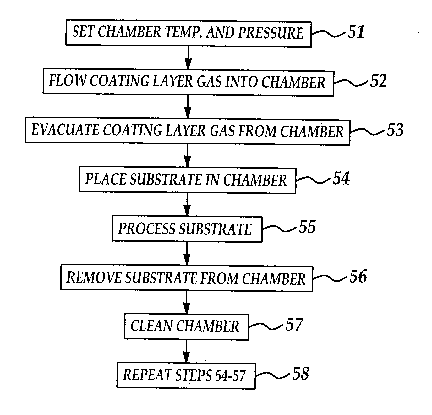
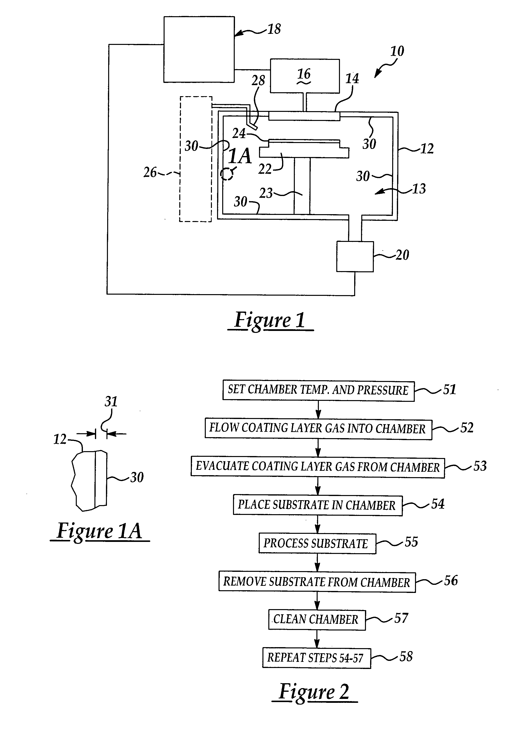
[0026] The present invention has particularly beneficial utility in the cleaning of physical vapor deposition (PVD) chambers used to deposit a silicon-containing layer on a high-k dielectric layer in the fabrication of a gate stack, particularly in MOSCAP (metal oxide semiconductor capacitor) structures and MOSFET (metal oxide semiconductor field effect transistor) structures on semiconductor wafer substrates. However, the invention is not so limited in application and is equally applicable to semiconductor IC fabrication processes in general as well as other industrial processes.

[0027] The present invention is generally directed to a method which includes providing a repellant coating layer on the interior surfaces of a process chamber to prevent residial etchant chamber cleaning chemicals or agents from remaining in the chamber after periodic chamber cleanings carried out to remove material deposits from the interior surfaces of the chamber. The repellant coating layer has a hydr...


PUM

PropertyMeasurementUnit
Thicknessaaaaaaaaaa
Thicknessaaaaaaaaaa
Thicknessaaaaaaaaaa

Abstract

A method for cleaning a process chamber in such a manner that chamber-cleaning chemicals or agents are incapable of remaining in the chamber after cleaning and chemically interfering with semiconductor fabrication or other processes subsequently carried out in the chamber. The method includes providing a repellant coating layer having a hydrophobic or hydrophilic polarity on the interior surfaces of a process chamber and using a cleaning agent having a polarity opposite that of the repellant coating layer to clean the chamber. Accordingly, the cleaning agent removes post-processing chemical residues from the interior chamber walls and other surfaces and is incapable of adhering to the surfaces and remaining in the chamber upon commencement of a subsequent process carried out in the chamber.

Description

FIELD OF THE INVENTION [0001] The present invention relates to chemical vapor deposition (CVD) technology used in the deposition of material layers such as polysilicon in the fabrication of polygates on a semiconductor wafer substrate. More particularly, the present invention relates to a novel method for the cleaning of a CVD chamber to prevent residual HCl chamber cleaning gas from remaining in the chamber and rendering silicon unstable in the fabrication of a polygate stack on a high-k dielectric material. BACKGROUND OF THE INVENTION [0002] The fabrication of various solid state devices requires the use of planar substrates, or semiconductor wafers, on which integrated circuits are fabricated. The final number, or yield, of functional integrated circuits on a wafer at the end of the IC fabrication process is of utmost importance to semiconductor manufacturers, and increasing the yield of circuits on the wafer is the main goal of semiconductor fabrication. After packaging, the cir...

Claims


Application Information

Patent Timeline
IPC IPC(8): B08B7/00C23C16/00C23C16/44
CPCB08B7/0035C23C16/4405C23C16/4404
Inventor YANG, MING-HOYAO, LIANG-GEICHEN, SHIH-CHANG
Owner TAIWAN SEMICON MFG CO LTD
Why Eureka
Try Eureka