Polishing composition and polishing method

a technology of polishing composition and composition, applied in the field of polishing composition, can solve the problems of variant stock removal rate significant deterioration in the preliminary polishing step,

Active Publication Date: 2005-09-29
FUJIMI INCORPORATED
View PDF29 Cites 15 Cited by
  • Summary
  • Abstract
  • Description
  • Claims
  • Application Information

AI Technical Summary

Benefits of technology

[0005] It is an object of the present invention to provide a polishing composition that can be suitably used in polishing for forming conducti...

Problems solved by technology

When the polishing composition for the finish polishing step is mixed into the polishing composition for the preliminary polishing step, a protective film is formed on the conductive layer by the action of the agent for forming a protective film in the polishing composition for the finish polishing step, causing a significant d...

Method used


Image

  • Polishing composition and polishing method
  • Polishing composition and polishing method

Examples


Embodiment Construction

[0011] One embodiments of the present invention will now be described.

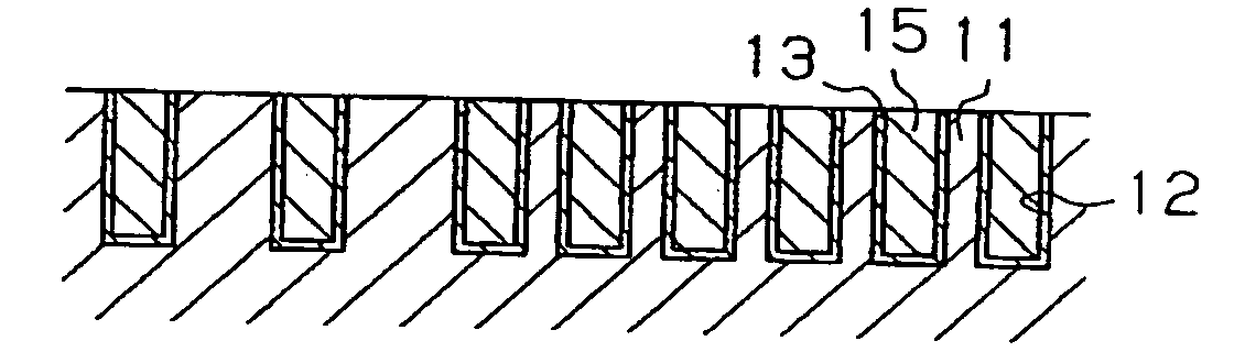
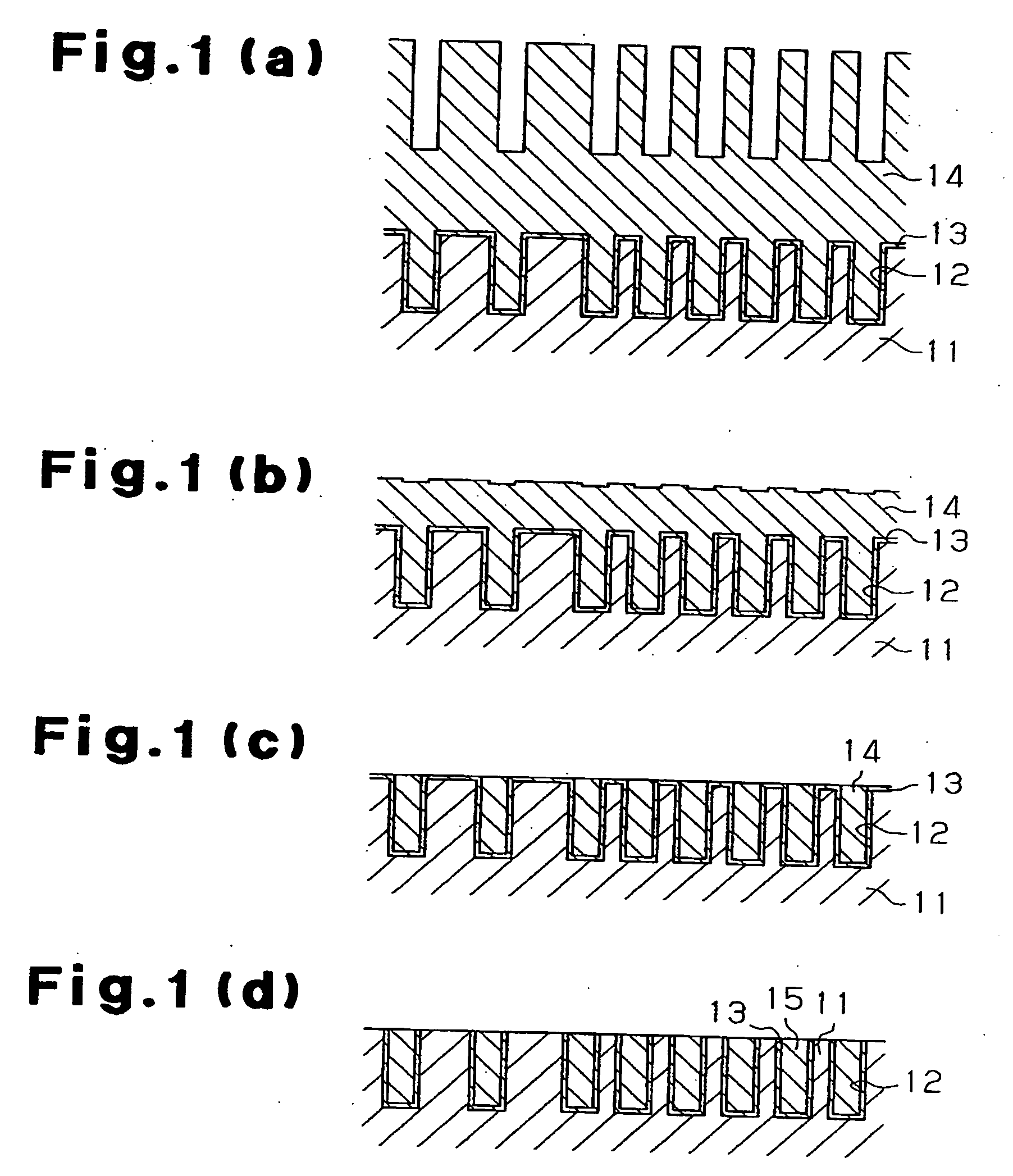
[0012] First, a method for forming conductive wiring in a semiconductor device will be described. In forming conductive wiring in a semiconductor device, as illustrated in FIG. 1(a), a barrier film 13 and a conductive film 14 are first formed on an insulating film 11 having trenches 12.

[0013] The insulating layer 11 may be made of SiO2, SiOF or SiOC. The insulating layer 11 is formed by the Chemical Vapor Deposition (CVD) using tetraethoxy silane (TEOS), borosilicate glass (BSG), phosphosilicate glass (PSG) or boron phosphosilicate glass (BPSG). The trenches 12 are formed for example by the known lithography and pattern etching techniques so as to have a prescribed design pattern.

[0014] The barrier layer 13 is formed on the insulating layer 11 so as to cover the surface thereof in advance of formation of the conductive layer 14, serves to prevent metal atoms in the conductive layer 14 from diffusion in the insu...


PUM


Abstract

A polishing composition contains a deterioration inhibitor for inhibiting deterioration of polishing capability of the polishing composition, an abrasive, and water. The deterioration inhibitor is at least one selected from polysaccharide and polyvinyl alcohol. The polysaccharide is starch, amylopectin, glycogen, cellulose, pectin, hemicellulose, pullulan, or elsinan. Among them, pullulan is preferable. The abrasive is at least one selected from aluminum oxide and silicon dioxide, preferably at least one selected from fumed silica, fumed alumina, and colloidal silica. The polishing composition can be suitably used in polishing for forming wiring a semiconductor device.

Description

BACKGROUND OF THE INVENTION [0001] The present invention relates to a polishing composition for use, for example, in polishing for forming conductive wiring in a semiconductor device, and a polishing method using such a polishing composition. [0002] Conductive wiring in a semiconductor device is at present mainly produced by a damascene process, which is based on a chemical mechanical polishing (CMP) technique. For producing conductive wiring, trenches are first formed on an insulating layer of insulating material (e.g., SiO2), provided on a semiconductor board. Next, a conductive layer of conductive metal (e.g., Cu) is provided on the insulating layer so as to at least fill up the trenches. Then, the portion of the conductive layer, which is positioned outside the trenches, is removed by polishing. As a result, the portion of the conductive layer, which is positioned in the trenches, remains on the insulating layer acts as conductive wiring. [0003] Polishing for removing the portio...

Claims


Application Information

Patent Timeline
IPC IPC(8): B24B37/00C09G1/02C09K3/14H01L21/00H01L21/304H01L21/321
CPCC09G1/02H01L21/3212C09K3/1463C09K3/14
Inventor OH, JUNHUIKAWAMURA, ATSUNORIMATSUDA, TSUYOSHIHIRANO, TATSUHIKOSAKAI, KENJIHORI, KATSUNOBU
Owner FUJIMI INCORPORATED
Why Eureka
Try Eureka