Transmitter

a transmitter and receiver technology, applied in the field of radio transmitters, can solve problems such as deterioration of evms, and achieve the effect of high efficiency of operation

Inactive Publication Date: 2005-09-29
PANASONIC CORP
View PDF6 Cites 50 Cited by
  • Summary
  • Abstract
  • Description
  • Claims
  • Application Information

AI Technical Summary

Benefits of technology

[0017] An object of the present invention is to provide a transmitter that can achieve a broadband EER method, without reducing efficiency.
[0019] According to this configuration, there is provided the first and the second plurality of switching regulators that convert the supply voltage into the plurality of voltages whose values are stepwisely different, any one of the output voltages of the first plurality of switching regulators is selected by the first switch group according to levels of the amplitude component, and the amplitude amplifying means uses the output voltage of the selected switching regulator as the supply voltage. In addition, any one of the output voltages of the second plurality of switching regulators is selected by the second switch group according to the levels of the amplitude component, and the linear DC converting means performs the DC conversion of the amplitude component using the output voltage of the selected switching regulator as the supply voltage. Therefore, a voltage drop due to the linear DC converting means can be suppressed to be low, and a power loss due to the linear DC converting means can be suppressed. Moreover, since the amplitude amplifying means can also be driven with the minimum voltage in order to linearly amplify the amplitude component, power consumption can be suppressed to be low. Accordingly, a consumed electric current of a circuit block which performs analog operation of the amplitude component can be suppressed to be low. In addition, the linear DC converting means is used for the DC conversion, thereby making it possible to achieve broadband. Accordingly, a broadband EER method can be achieved, without reducing the efficiency.
[0020] Further, when not the phase component but the modulated signal is used as it is, it is possible to avoid a deterioration of a modulation accuracy (Error Vector Magnitude: EVM), which can not be avoided in the EER method that separates the signal into the amplitude component and the phase component and extracts them. In other words, when using the phase component, the phase component is filtered within the range that a band of an digital-to-analog converter allows, and to the extent of not affecting the EVM. At this time, a partial level drop of the phase component caused by the filtering has caused a remarkable deterioration of the EVM, when the phase component has been composed with the amplitude component at an output of the RF power amplifier. In addition, since as compared with the phase component separated from the modulated signal, a necessary bandwidth of the modulated signal is smaller by about 1 / 6, a bandwidth of a digital-to-analog converter and a bandwidth of an anti-aliasing filter which suppresses a spurious component produced by digital-to-analog conversion can be narrowed. Therefore, it is advantageous to achieve a reduction in power consumption of the digital-to-analog converter, and a miniaturization and a reduction in cost of the an inductor being used for the filter.
[0024] According to this configuration, there is provided the first and the second plurality of switching regulators that convert the supply voltage into the plurality of voltages whose values are stepwisely different, the plurality of linear DC converting means perform the DC conversion of the amplitude component, respectively, using the output voltage of the second plurality of switching regulators as the supply voltage, and any one of the plurality of linear DC converting means is made selectively effective according to the levels of the amplitude component. Therefore, a voltage drop by the linear DC converting means when performing the DC conversion can be suppressed to be low, and the power loss by the linear DC converting means can also be suppressed to be low. Further, since any one of the output voltages of the first plurality of switching regulators is also selected according to the levels of the amplitude component for the amplitude amplifying means, it can be driven with the minimum voltage in order to linearly amplify the amplitude component. Therefore, the power consumption can be suppressed to be low. In addition, the linear DC converting means is used for the DC conversion, thereby making it possible to achieve broadband. Accordingly, the broadband EER method can be achieved, without reducing the efficiency. In addition, since the linear DC converting means is only provided between the switching regulator and the RF power amplifier, and the second switching means is removed from the path, the power loss can further be reduced.
[0026] According to this configuration, following function and effect may be provided. Since the band of the phase amplitude separating means is hundreds of MHz at most, when a carrier exceeds GHz, the transmitter can not deal with this frequency, but by using, for example an quadrature modulator which is the frequency converting means, a carrier frequency can easily be up-converted.
[0027] As explained in detail in the above, according to the present invention, in the EER method which allows the RF power amplifier to operate as the saturated type amplifier, a broadband and highly efficient operation can be achieved.

Problems solved by technology

At this time, a partial level drop of the phase component caused by the filtering has caused a remarkable deterioration of the EVM, when the phase component has been composed with the amplitude component at an output of the RF power amplifier.

Method used


Image

  • Transmitter
  • Transmitter
  • Transmitter

Examples


first embodiment

[0034] Hereafter, a first embodiment of the present invention will be explained with reference to the drawing. In this embodiment, a wireless LAN system according to IEEE802.11a standard which uses a broadband modulated signal will be explained as an example.

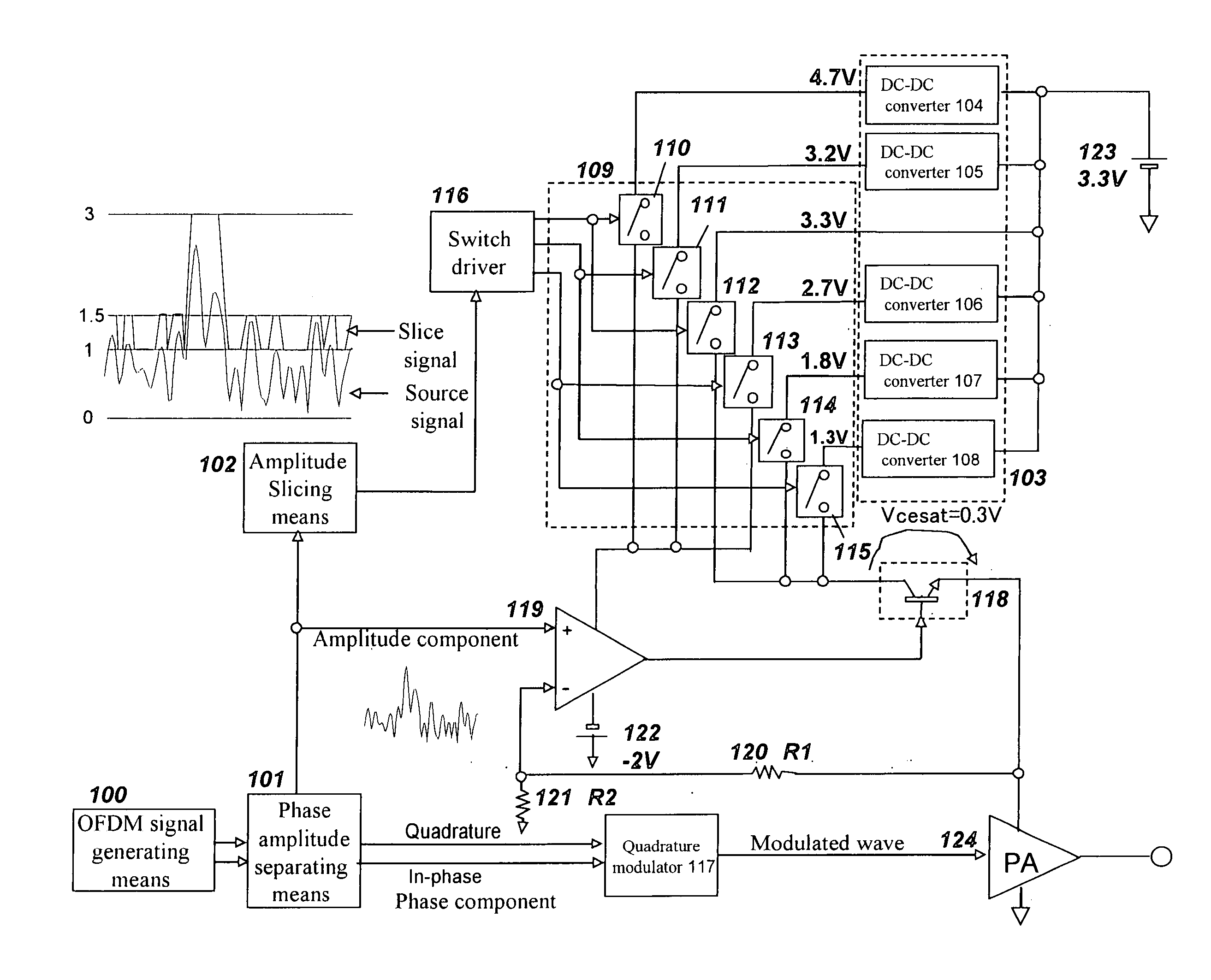
[0035]FIG. 1 shows a circuit diagram of a transmitter according to the first embodiment of the present invention which achieves an EER method. As shown in FIG. 1, this transmitter includes an OFDM signal generating means 100, a phase amplitude separating means 101, an amplitude slicing means 102, a switching regulator group 103, a switch group 109, a switch driver 116, an quadrature modulator 117, an emitter follower 118, an operational amplifier 119, a resistor 120 with a resistance R1, a resistor 121 with a resistance R2, a negative power supply 122 with a negative voltage of −2 V, a positive power supply 123 with a positive voltage of 3.3V, and a saturated type RF power amplifier 124.

[0036] The above OFDM signal generating ...

second embodiment

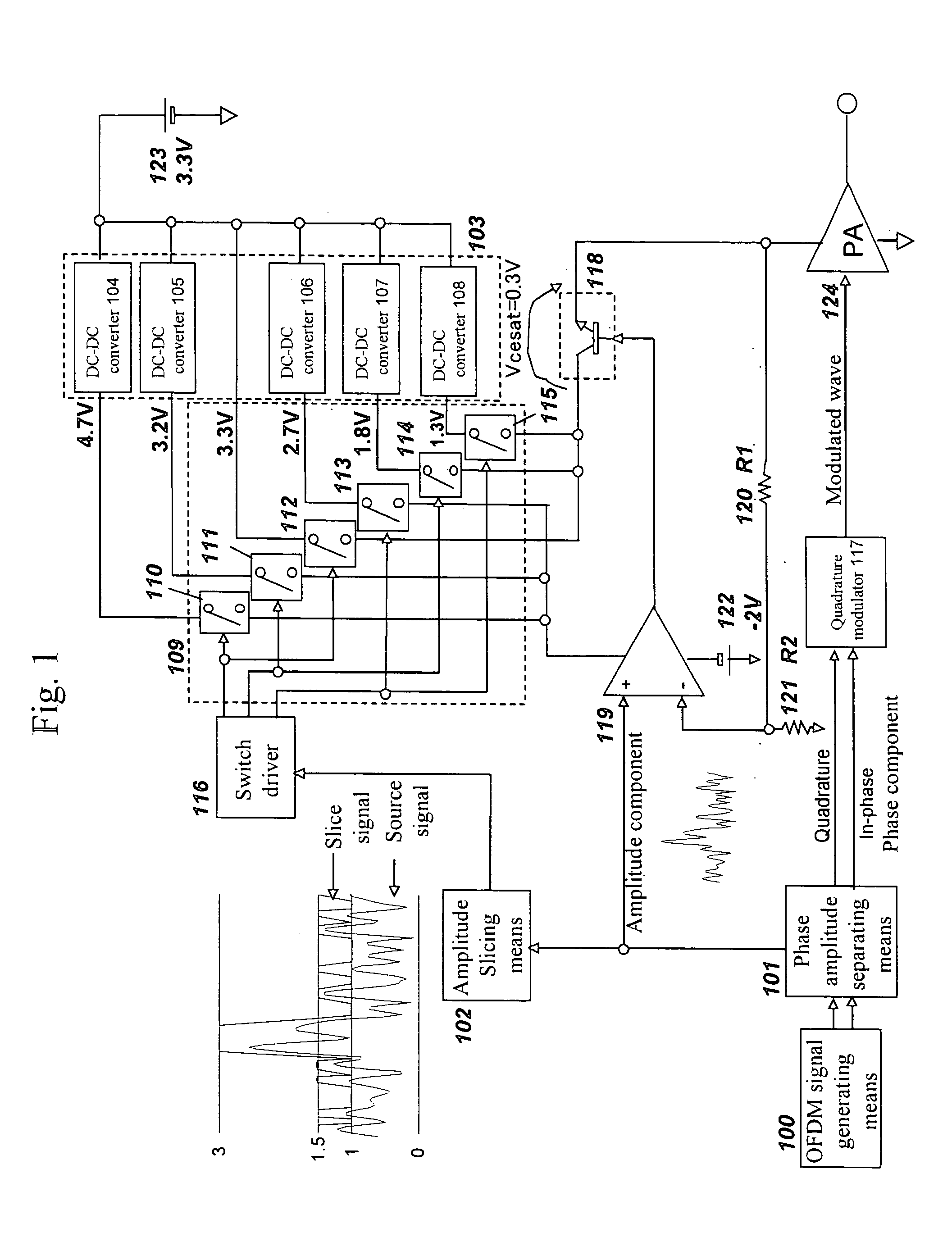
[0098]FIG. 2 is a block diagram of a transmitter according to a second embodiment of the present invention. This embodiment is different from the first embodiment with respect to the followings. That is, the outputs from the positive power supply 123 and the DC-DC converters 107 and 108 are directly connected the collectors of respective emitter followers 201 through 203 of an emitter follower group 200 of the same number as that of those outputs. In addition, paths connected to base terminals of respective emitter followers 201 through 203 of this emitter follower group 200 are switched by switches the 112, 114, and 115, the number of which is the same as that of the emitter followers 201 through 203 of the emitter follower group 200. The same symbol is given to the same component as that of the first embodiment and description thereof will be omitted.

[0099] A base current of the specific emitter follower among the emitter followers 201 through 203 of the emitter follower group 20...

third embodiment

[0101]FIG. 3 is a block diagram of a transmitter according to a third embodiment of the present invention. This embodiment is different from the first embodiment with respect to the followings. That is, an output of the OFDM signal generating means 100 is outputted to the quadrature modulator 117. The output of the OFDM signal generating means 100 is also inputted into an amplitude extracting means 300. The amplitude component extracted by the amplitude extracting means 300 is outputted to the operational amplifier 119 and the amplitude slicing means 102. The same symbol is given to the same component as that of the first embodiment and description thereof will be omitted.

[0102] As for additional effects expected for the third embodiment, since not the phase component but the modulated signal is provided to the RF power amplifier 124 via the quadrature modulator 117 as it is, it is possible to avoid the deterioration of the modulation accuracy (Error Vector Magnitude: EVM), which c...


PUM


Abstract

An amplitude component and a phase component of a modulated signal are inputted into a power supply terminal and an input terminal of an RF power amplifier, respectively, and a modulated wave that is produced by demodulating an original modulated signal is obtained from the RF power amplifier. A supply voltage is supplied to an emitter follower and an operational amplifier via a switch group from a DC-DC converter group whose output voltages are sequentially different. As the supply voltage, any pair of outputs of DC-DC converters by the switch group is selected according to levels of the amplitude component, and provides them to the emitter follower and the operational amplifier. The emitter follower performs a DC conversion of the provided supply voltage to provide it to the RF power amplifier.

Description

BACKGROUND OF THE INVENTION [0001] 1. Field of the Invention [0002] The present invention relates to a radio transmitter being used for a communication mode which uses a multicarrier signal, such as OFDM (Orthogonal Frequency Division Multiplex) scheme. [0003] 2. Description of the Prior Art [0004] Generally, to process a signal modulated with an amplitude modulation scheme, especially a signal modulated with a multi-level modulation scheme, such as a quadrature amplitude modulation (hereinafter, referred also to as QAM) scheme, a linear amplification is required to an RF power amplifier for transmitting power to an antenna. For that reason, class A or class AB has been adopted as an operation class of the RF power amplifier. [0005] However, with the progress of broadband communications, a communication mode using a multicarrier signal, such as an Orthogonal Frequency Division Multiplex (hereinafter, referred also to as OFDM) scheme has come to be used. However, when using a convent...

Claims


Application Information

Patent Timeline
Patent Type & Authority Applications(United States)
IPC IPC(8): H04J11/00H01Q11/12H03F1/02H03F1/32H03F3/38H04B1/02H04B1/04
CPCH03F1/0211H03F1/0227H04B2001/045H03F1/32H03F2200/511H03F1/0277H03F1/02H03F3/24
Inventor TANABE, MITSURUAKIZUKI, TAIJITANAKA, KOICHIRO
Owner PANASONIC CORP
Why Eureka
Try Eureka