Nanoengineered thermal materials based on carbon nanotube array composites

a carbon nanotube and composite material technology, applied in nanoinformatics, electrical apparatus construction details, light and heating apparatus, etc., can solve the problems of increasing the difficulty of providing heat dissipation and transportation for such components and devices, increasing local power consumption, and increasing the mechanical strength of carbon nanotubes (cnts). , to achieve the effect of improving the mechanical strength of carbon nanotubes, reducing the cost of production and high thermal conductivity

Inactive Publication Date: 2005-10-13
SAMSUNG ELECTRONICS CO LTD +1
View PDF72 Cites 96 Cited by
  • Summary
  • Abstract
  • Description
  • Claims
  • Application Information

AI Technical Summary

Benefits of technology

[0008] These needs are met by the invention, which uses an embedded carbon nanotube array to provide one or more high performance thermal conductors for applications that require large heat dissipation. This approach also improves the mechanical strength of carbon nanotubes (CNTs) so that the CNT array can remain stable and can make good contact to the surface of objects that generate large amount of heat, through use of reversible buckling and bending of exposed portions of the CNTs. The extremely high thermal conductivity along a carbon nanotube axis is employed to transfer heat away from hot spots in a component or device. Copper and other high thermal conductivity materials are deposited to fill interstitial regions or gaps in a first part of a CNT array. This composite structure provides mechanical strength to maintain the CNTs in position and also serves as an efficient heat transfer material to improve diffusion of heat flux from an individual CNT to a larger surrounding volume.

Problems solved by technology

As the size of components and devices for ICs and other appliances becomes smaller, it becomes more difficult to provide heat dissipation and transport for such components and devices.
A thermal conductor for a macro size thermal conductor is generally inadequate for use with a micro size component or device, in part due to scaling problems.
One consequence of increased component density in, and compactness of, ICs manifests itself in the form of locally high power consumption.
The cooling of an object by attaching it to a cold reservoir is normally limited by the heat transfer rate across the interface.
Metal film can be used to improve the thermal conductivity but is only applicable for high pressure loading.

Method used


Image

  • Nanoengineered thermal materials based on carbon nanotube array composites
  • Nanoengineered thermal materials based on carbon nanotube array composites
  • Nanoengineered thermal materials based on carbon nanotube array composites

Examples


Embodiment Construction

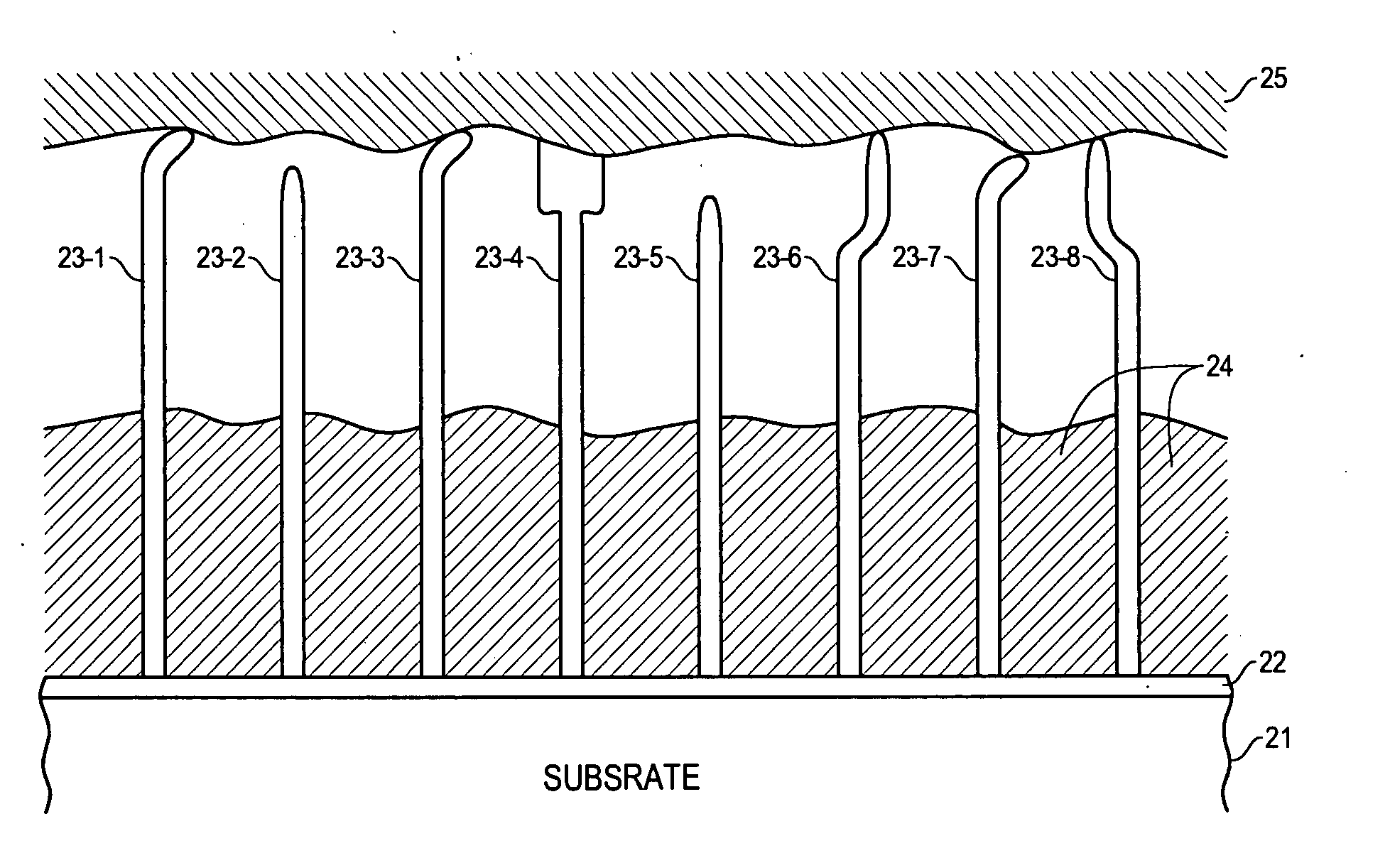
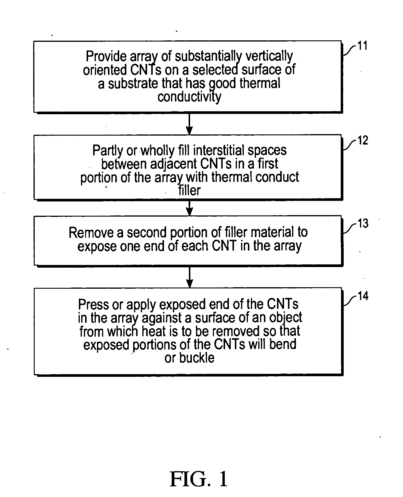
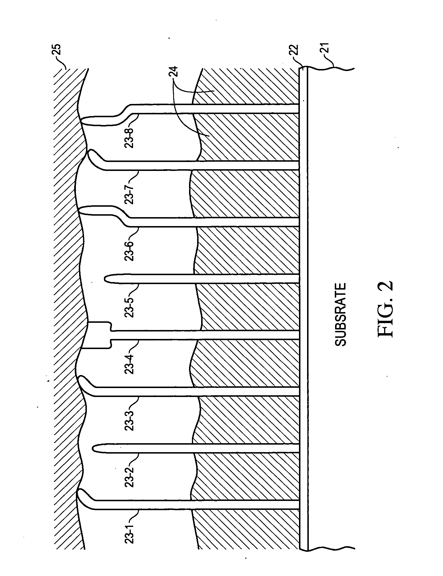
[0022]FIG. 1 illustrates a procedure for practicing an embodiment of the invention. In step 11, an array of substantially vertically oriented CNTs is grown on a selected surface of a substrate that has good thermal conductivity. The substrate may be a metal-doped silicide, a diamond film, or a metallic substance having a maximum electrical or thermal conductivity. Whether the array is patterned or not, it is preferable to provide a thin CNT catalyst layer (e.g., Ni, Fe, Co, Pd or Al or a combination thereof) having a layer thickness of 2-50 nanometers (nm), or more if desired. When the CNT is grown in an electrical field oriented substantially perpendicular to the selected substrate surface, the CNTs can be grown in greater lengths (1-50 μm or more) in a direction substantially parallel to the electrical field direction.

[0023] In step 12, interstitial spaces between adjacent CNTs are partly or fully filled with a selected filler material that is preferably a good thermal conductor ...


PUM

PropertyMeasurementUnit
lengthaaaaaaaaaa
thicknessaaaaaaaaaa
thicknessaaaaaaaaaa

Abstract

A method for providing for thermal conduction using an array of carbon nanotubes (CNTs). An array of vertically oriented CNTs is grown on a substrate having high thermal conductivity, and interstitial regions between adjacent CNTs in the array are partly or wholly filled with a filler material having a high thermal conductivity so that at least one end of each CNT is exposed. The exposed end of each CNT is pressed against a surface of an object from which heat is to be removed. The CNT-filler composite adjacent to the substrate provides improved mechanical strength to anchor CNTs in place and also serves as a heat spreader to improve diffusion of heat flux from the smaller volume (CNTs) to a larger heat sink.

Description

CROSS REFERENCE TO RELATED APPLICATIONS [0001] This application claims the benefit of U.S. patent application Ser. No. ______(ARC-15042-1), which is incorporated by reference herein.ORIGIN OF THE INVENTION [0002] The invention described herein was made by employees of the United States Government and may be manufactured and used by or for the Government for governmental purposes without the payment of any royalties thereon or therefor.TECHNICAL FIELD [0003] The present invention provides thermal conductors for small components and devices, using carbon nanotube arrays. BACKGROUND OF THE INVENTION [0004] State-of-the-art integrated circuits (ICs) for microprocessors routinely dissipate power densities on the order of 50 Watts / cm2. This large power is due to the localized heating of ICs operating at high frequencies, and must be managed for future high-frequency microelectronic applications. As the size of components and devices for ICs and other appliances becomes smaller, it becomes...

Claims


Application Information

Patent Timeline
Patent Type & Authority Applications(United States)
IPC IPC(8): H01L23/373H05K7/20
CPCB82Y10/00B82Y30/00H01L23/373H01L2224/16H01L2224/73253H01L2924/01046H01L2924/01078H01L2924/01079H01L2924/15312H01L2924/01019H01L2924/01322B82Y40/00F28F13/00
Inventor LI, JUNMEYYAPPAN, MEYYA
Owner SAMSUNG ELECTRONICS CO LTD
Why Eureka
Try Eureka