Mounting substrate and mounting method of electronic part
a technology of mounting substrate and electronic parts, which is applied in the direction of printed circuit non-printed electric components association, sustainable manufacturing/processing, and final product manufacturing, etc., can solve the problems of degrading the reliability of the solder connection, further and affecting the reliability of the connection
- Summary
- Abstract
- Description
- Claims
- Application Information
AI Technical Summary
Benefits of technology
Problems solved by technology
Method used
Image

Examples
first embodiment
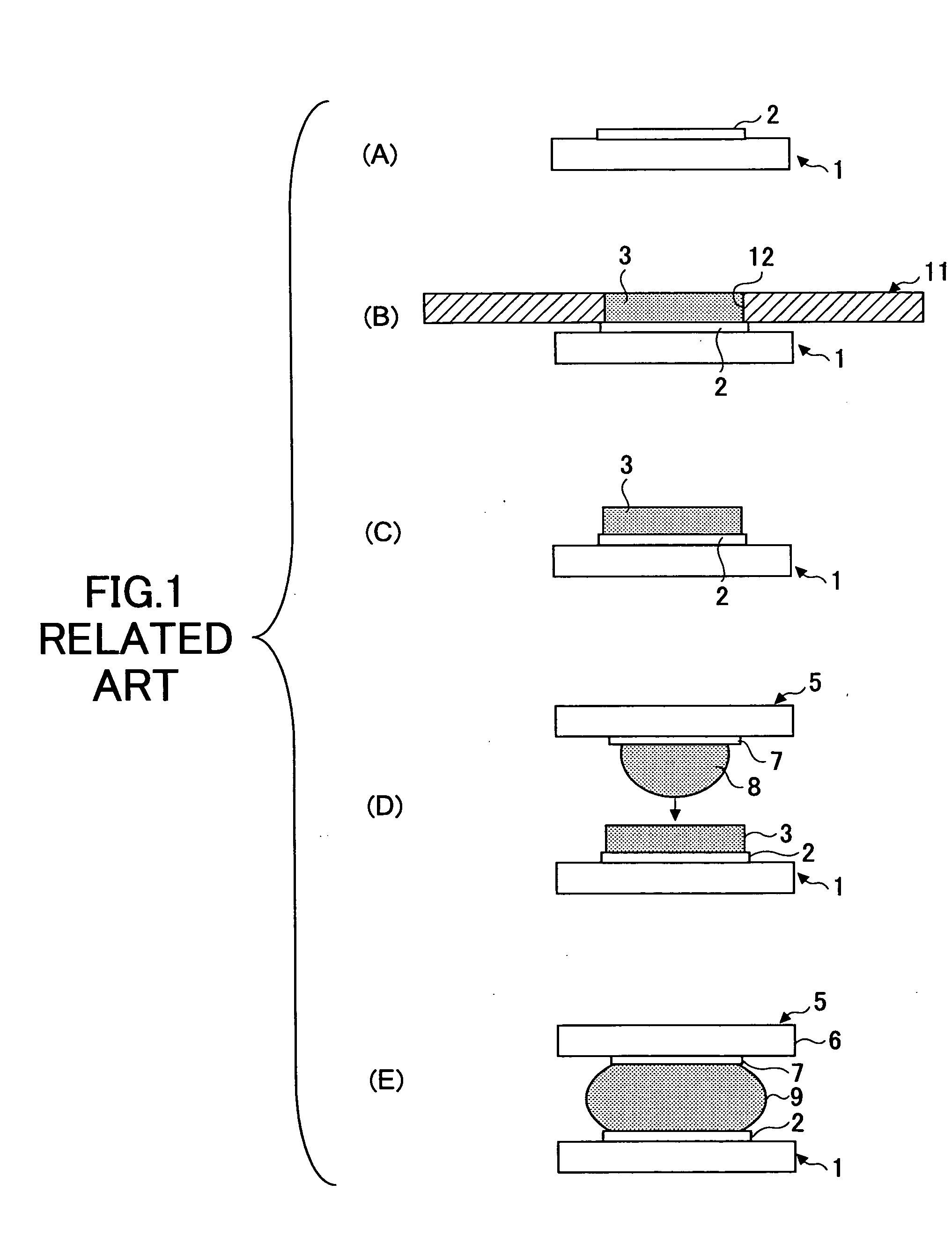
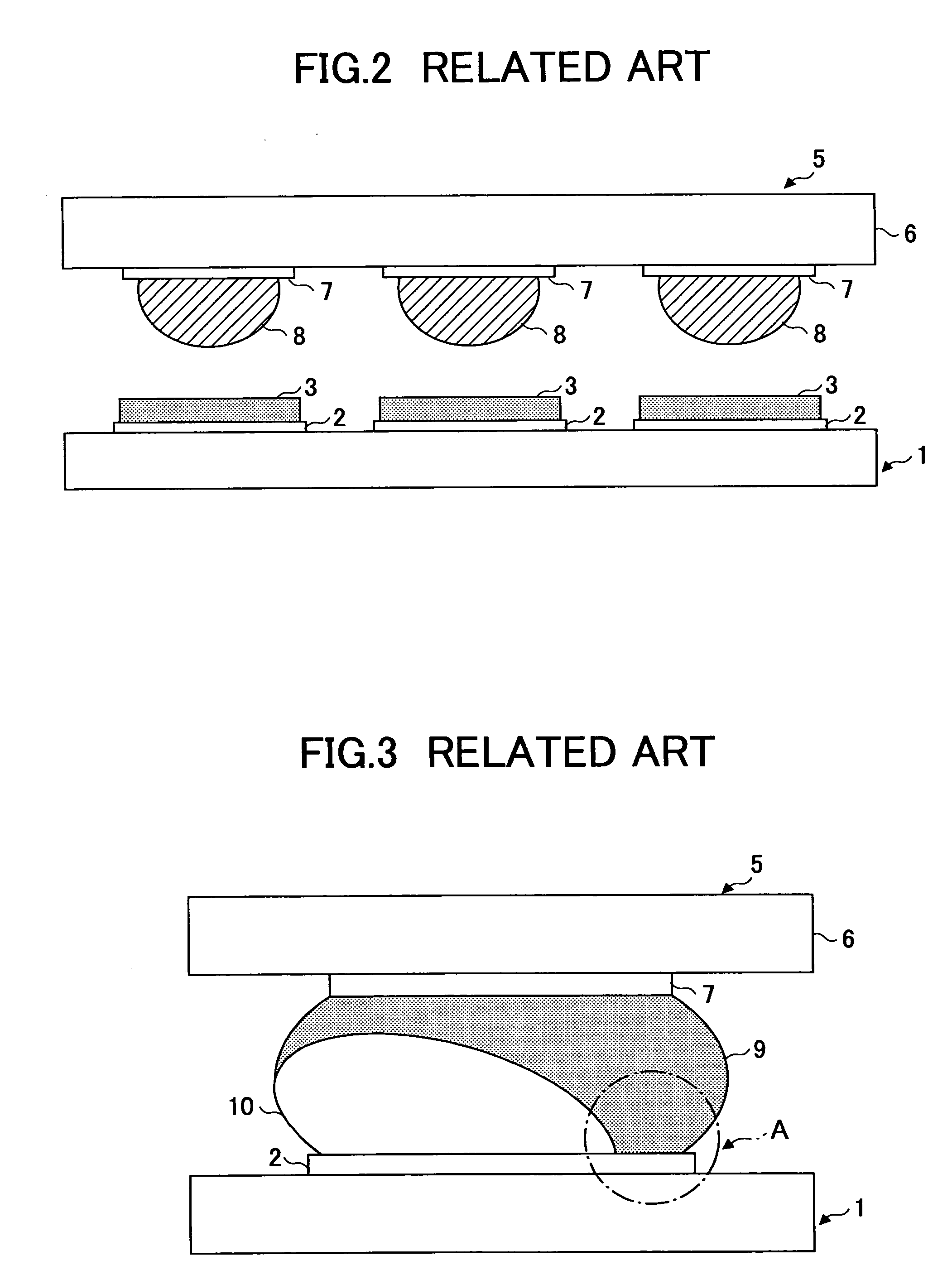
[0092]FIG. 4 is a process view for explaining the present invention. FIG. 4 shows a method for connecting an electronic part 25 to a mounting substrate 20 by using a melt-capable connection member. In the below embodiments, solder is used as an example of the melt-capable connection member. The melt-capable connection member of the present invention is a melt-capable material having conductivity and functions for connecting an electrode of the electronic part and a land of the mounting substrate. The solder (Sn—Pb eutectic solder, lead free solder such as Sn—Ag—Cu solder, a solder paste, or the like), resin where a metal such as Sn, Au, Ag, and others, a solder material, or a conductive metal powder is mixed, or the like, can be used as a concrete material of the melt-capable connection member.
[0093] As shown in FIG. 4-(D), the electronic part 25 is a semiconductor device, for example. The electronic part 25 has a structure where a solder ball 28 is formed on a part side land 27 on ...
second embodiment
[0106]FIG. 6 shows the present invention.
[0107] In FIG. 6 and FIGS. 7 through 18 which are used for explaining other embodiments, parts that are the same as the parts shown in FIGS. 4 and 5 are given the same reference numerals, and explanation thereof is omitted.
[0108] In the above-discussed first embodiment, the metal member 24 is used as the connection member flow generation part configured to make a flow at the molten solder 29A. On the other hand, in the second embodiment, a metal film 33 is provided as the connection member flow generation part configured to make a flow at the molten solder 29A. The metal film 33 is formed on the substrate side land 22 by using a plating method or a thin film forming technology such as a vaporization method.
[0109] This metal film 23, as well as metal member 24, is formed by a material having a wettability lower than a material of the substrate side land 22. For example, when Cu is used for the substrate side land 22, Sn, Ag, Bi, or the like ...
third embodiment
[0112]FIG. 8 shows the present invention.
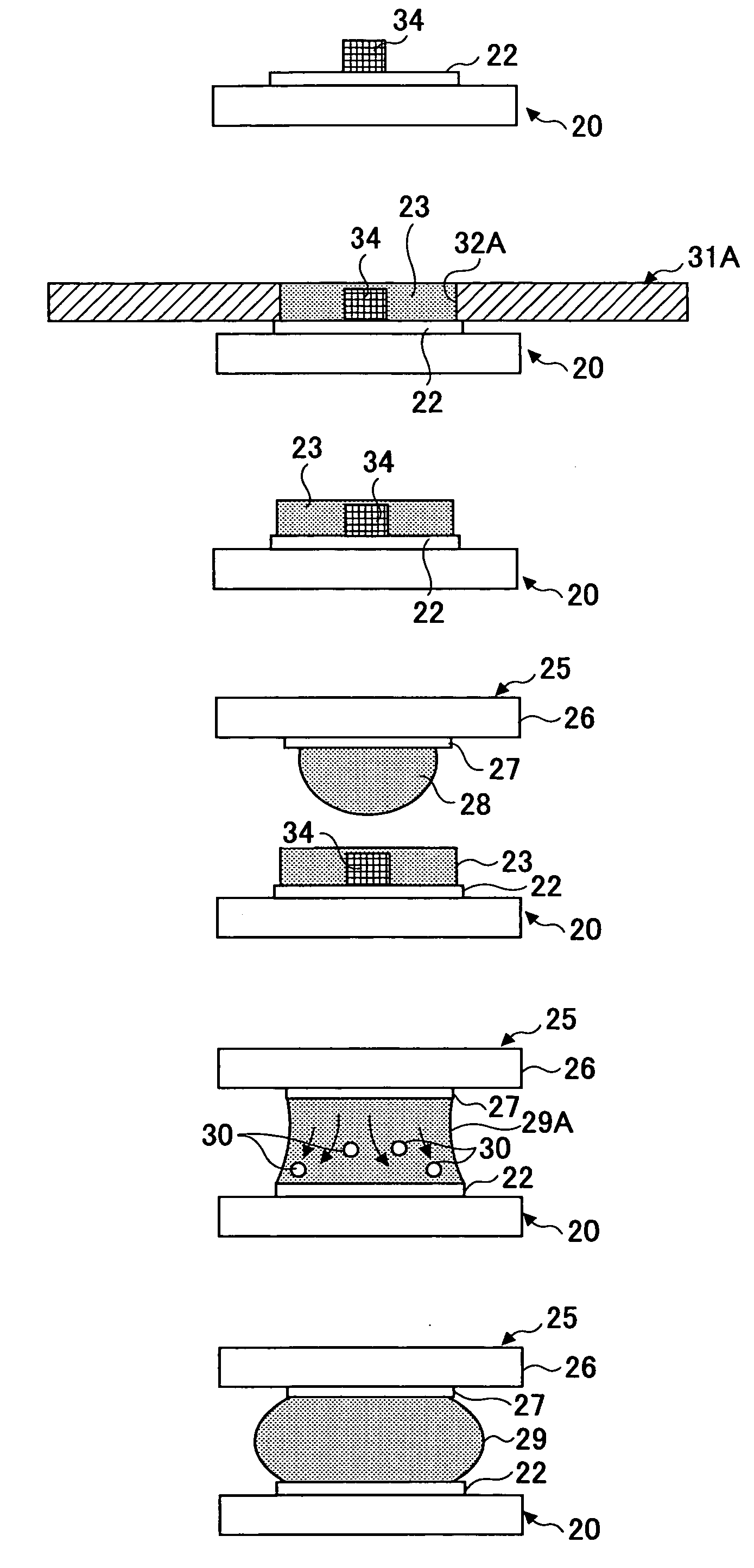
[0113] In the above-discussed first embodiment, the metal member 24 is used as the connection member flow generation part configured to make a flow at the molten solder 29A. On the other hand, in the third embodiment, a rosin 34 is provided as the connection member flow generation part configured to make a flow at the molten solder 29A.
[0114] The rosin 34 is resin of a tree such as a pine. The rosin has a melting point (liquid phase temperature) of approximately 90-100° C. which is lower than the melting point of the solder.
[0115] In this embodiment, in order to mount the electronic part 25 on the mounting board 20, first, as shown in FIG. 8-(A), the rosin 34 is provided on a substantially center part of the substrate side land 22 formed on the mounting board 20. In this example, the block-shaped rosin 34 is provided on the substrate side land 22. Since the rosin 34 has some degree of viscosity, the rosin 34 is provisionally fixed to the su...
PUM
| Property | Measurement | Unit |
|---|---|---|
| Length | aaaaa | aaaaa |
| Length | aaaaa | aaaaa |
| Fraction | aaaaa | aaaaa |
Abstract
Description
Claims
Application Information
 - R&D
- Intellectual Property
- Life Sciences
- Materials
- Tech Scout
- Unparalleled Data Quality
- Higher Quality Content
- 60% Fewer Hallucinations
Browse by: Latest US Patents, China's latest patents, Technical Efficacy Thesaurus, Application Domain, Technology Topic, Popular Technical Reports.
© 2025 PatSnap. All rights reserved.Legal|Privacy policy|Modern Slavery Act Transparency Statement|Sitemap|About US| Contact US: help@patsnap.com