

Semiconductor device, manufacturing process thereof and imaging device
a semiconductor and manufacturing process technology, applied in the direction of transistors, television systems, radio control devices, etc., can solve the problems of reducing the sensitivity of cmos image sensors and hardly ensuring the focal length in accordance with the thickness of the chip
- Summary
- Abstract
- Description
- Claims
- Application Information
AI Technical Summary
Benefits of technology
Problems solved by technology
Method used
Image

Examples
first embodiment
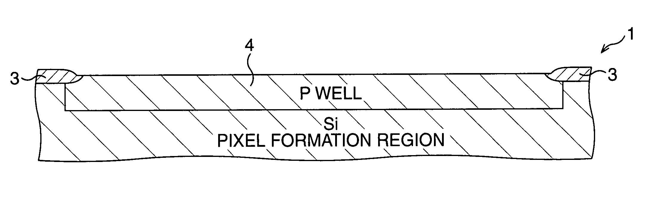
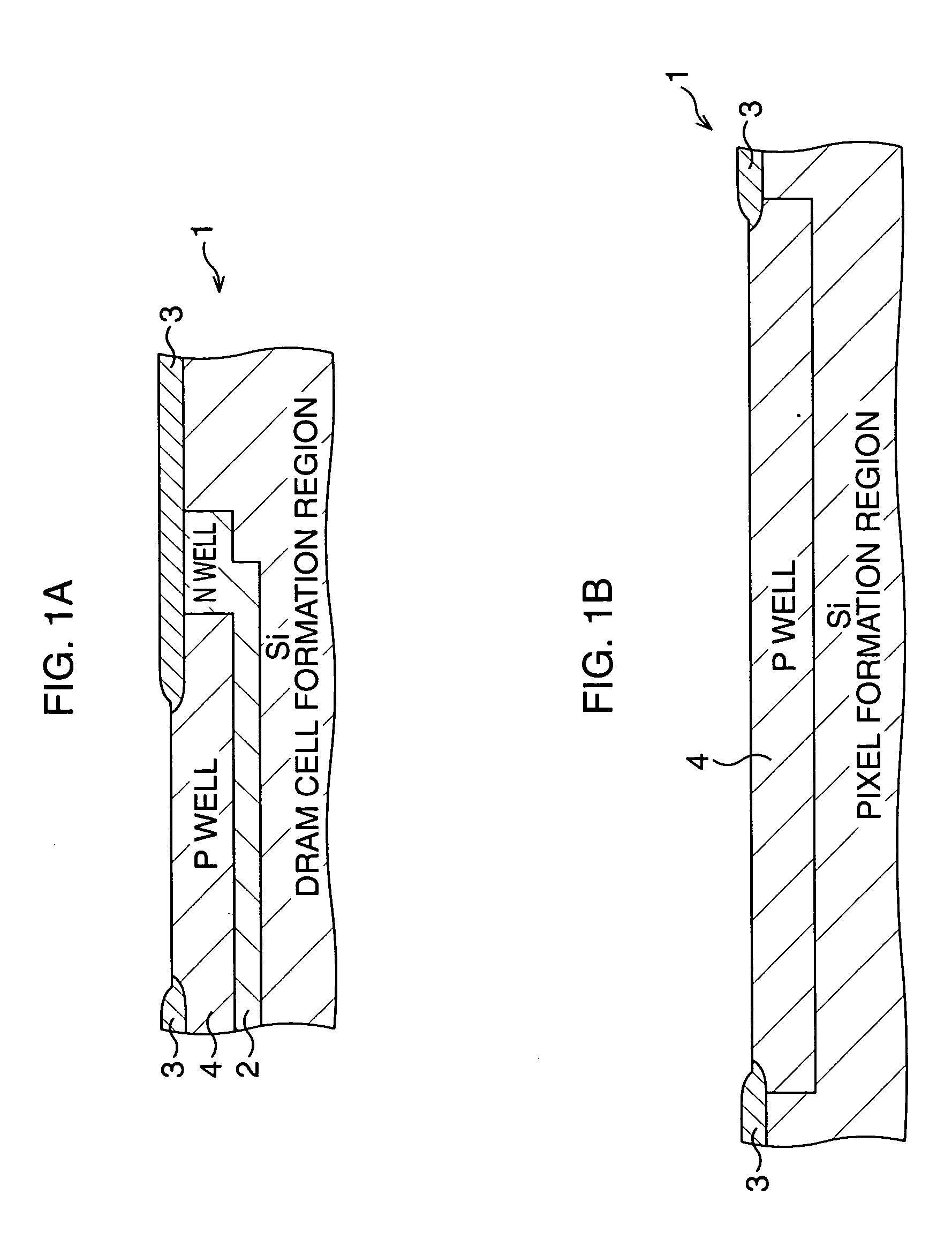
[0073] First of all, a manufacturing process of a CMOS image sensor packaged with DRAM according to the present invention will be described with reference to FIG. 1 to FIG. 15. In FIG. 1A to FIG. 12B, a manufacturing process of a DRAM cell formation region and a pixel formation region in the CMOS image sensor packaged with DRAM will be shown together.
[0074] As shown in FIG. 1A, an N-type well 2 is formed selectively in a DRAM cell formation region on a P-type Si substrate 1. Here, phosphorous or arsenic is ion implanted with a high energy to form the N-type well 2 to a deep level of the P-type Si substrate 1.
[0075] Then, as shown in FIG. 1A and FIG. 1B, a field oxide film 3 is formed by means of LOCOS, to define each of the element active regions such as a DRAM cell formation region, a pixel formation region and a periphery logic circuit formation region. Then, a P-type well 4 is formed to a shallow level in these elements active regions.
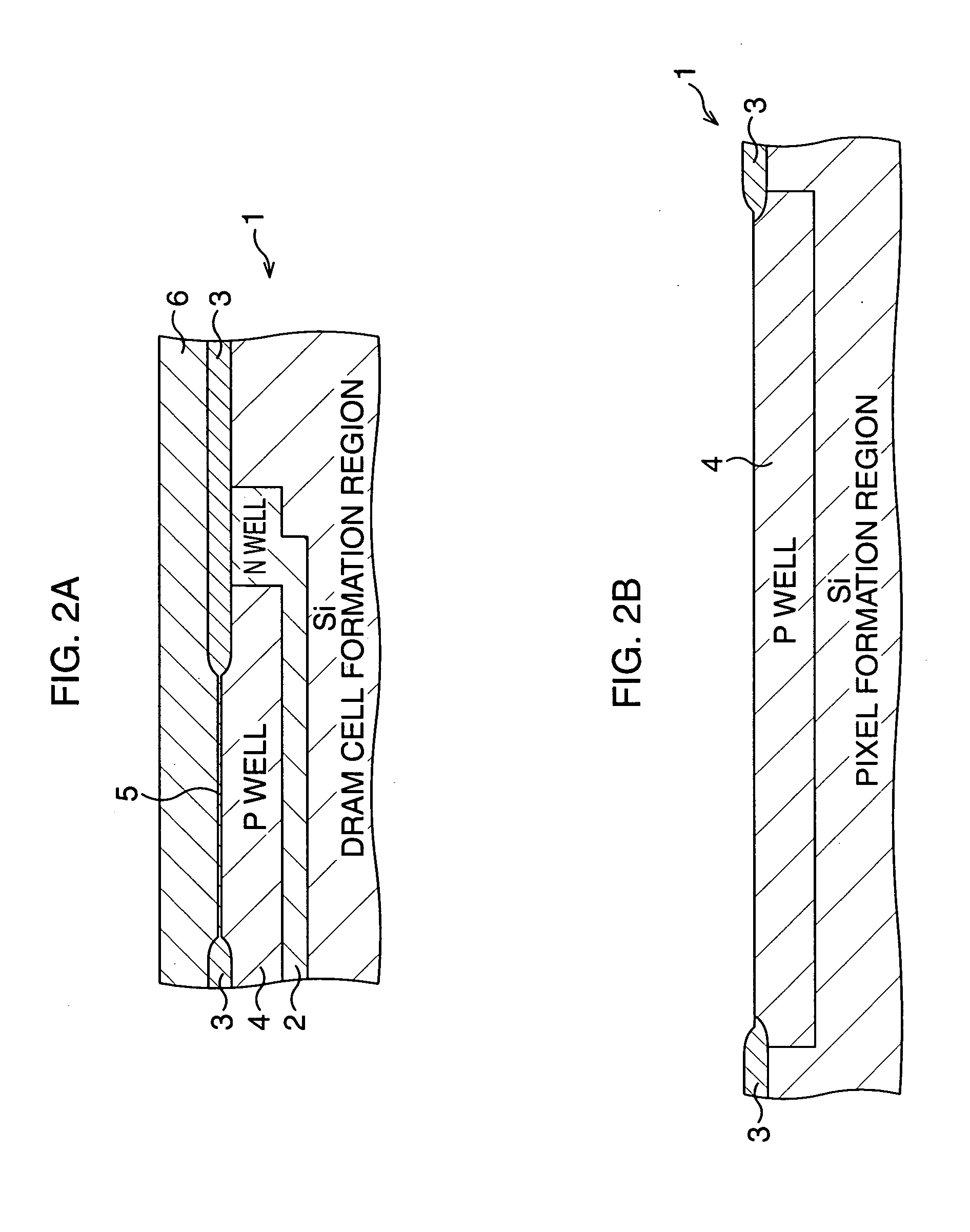
[0076] Then, as shown in FIG. 2A and FIG. 2...
second embodiment
[0115] Next, referring to FIG. 21A to FIG. 31, a manufacturing process of the CMOS image sensor packaged with DRAM according to the present invention will be described. In each of FIG. 21A to FIG. 28B, the manufacturing process of both of the DRAM cell formation region and the pixel formation region in the CMOS image sensor packaged with DRAM will be shown.
[0116] First of all, same as the example shown in FIG. 1A and FIG. 1B, an N-type well is formed selectively in a P-type Si substrate 47 in a DRAM cell formation region. Phosphorous or arsenic is ion implanted with a high energy to form an N-type well 48 to a deep level of the Si substrate 47.
[0117] Then, as shown in FIG. 21A, a trench capacitor of a substrate cell plate type is formed. The forming method of the trench capacitor is disclosed in, for example, “43rd Semiconductor Specialist Course Lectures”. A trench capacitor 53 is formed of a color oxide film, a SiN film 44, a polysilicon film 45 and a cell plate and the like. In ...
third embodiment
[0147] Next, referring to FIG. 32A to FIG. 42, a manufacturing process of a CMOS image sensor packaged with flash memory according to the present invention will be described. In each of FIG. 32A to FIG. 40, the manufacturing process of both of a flash memory cell formation region and a pixel formation region in the image sensor packaged with flash memory is shown.
[0148] First of all, same as the example shown in FIG. 1A and FIG. 1B, an N-type well 81 is formed selectively on a P-type Si substrate 80 in the flash memory cell formation region. Phosphorous or arsenic is ion implanted with a high energy to form the N-type well 81 to a deep level of the Si substrate 80.
[0149] Then, an STI 82 is formed to define element active regions of the flash memory cell formation region, a pixel formation region and a periphery logic circuit formation region respectively. Then, a P-type well 83 is formed to a shallow level of the respective element active regions.
[0150] Then, by means of thermal o...
PUM
 Abstract
Description
Claims
Application Information