High-K gate dielectric stack with buffer layer to improve threshold voltage characteristics

a buffer layer and dielectric stack technology, applied in the direction of electrical apparatus, semiconductor devices, dissimilar materials junction devices, etc., can solve the problems of difficulty in forming high-k gate dielectrics to achieve acceptable threshold voltage, reduced thickness of silicon dioxide layer, and limited success of proposed approaches. to achieve the effect of reducing the voltage threshold shi

Inactive Publication Date: 2005-10-13
TAIWAN SEMICON MFG CO LTD
View PDF12 Cites 169 Cited by
  • Summary
  • Abstract
  • Description
  • Claims
  • Application Information

AI Technical Summary

Benefits of technology

[0008] To achieve the foregoing and other objects, and in accordance with the purposes of the present invention, as embodied and broadly des...

Problems solved by technology

For example, the required thickness of a silicon dioxide layer decreases to less than about 20 Angstroms with concomitant problem of tunneling current leakage.
There have been, however, difficulties in forming high-k gate dielectrics to achieve acceptable threshold Voltage behavior in CMOS devices.
Proposed approaches so far have met with l...

Method used


Image

  • High-K gate dielectric stack with buffer layer to improve threshold voltage characteristics
  • High-K gate dielectric stack with buffer layer to improve threshold voltage characteristics
  • High-K gate dielectric stack with buffer layer to improve threshold voltage characteristics

Examples


Embodiment Construction

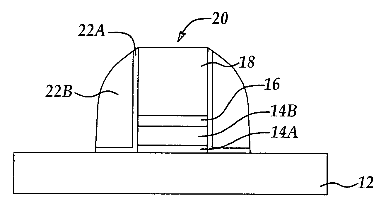
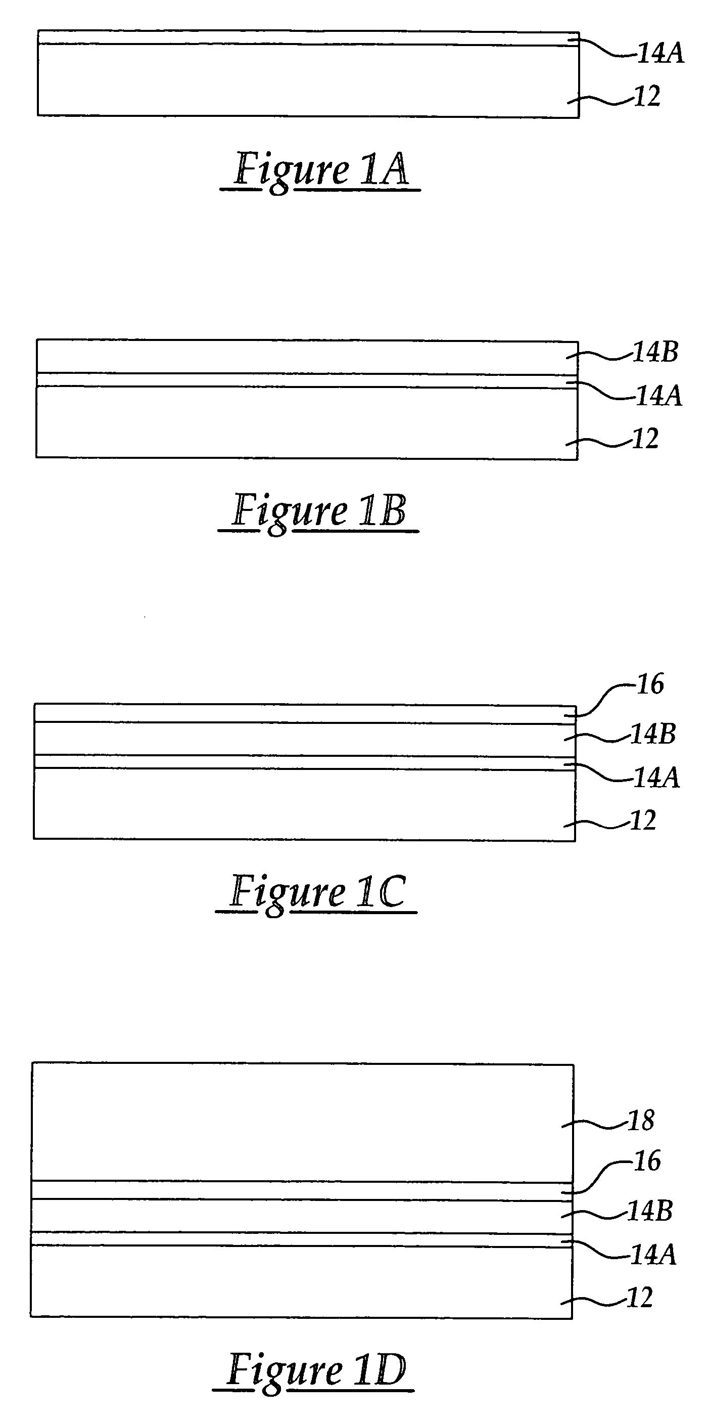
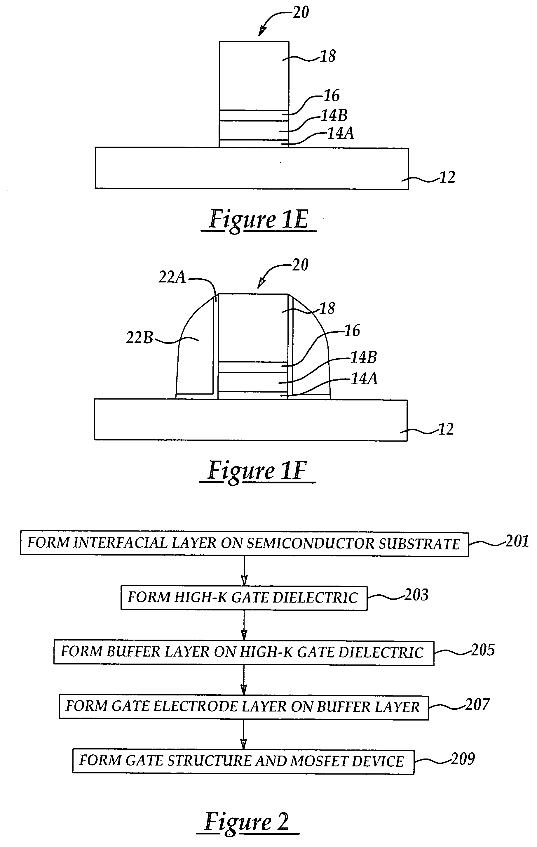
[0013] Embodiments of the present invention will now be described in detail with reference to the Figures where like numbered items refer to like structures wherever possible.

[0014] The gate structure and method for forming the same of the present invention is explained with respect to exemplary processing steps for forming deep submicron technology MOSFET devices, preferably having a characteristic (critical) dimension (e.g., gate length) less that about 90 nm. It will be appreciated that the method may be used with larger device characteristic dimensions, but that it is most advantageously used with deep sub-micron design rule technologies (e.g., equal to or less than about 90 nm.

[0015] In an exemplary embodiment of the present invention, reference is made to FIGS. 1A-1F where cross sectional schematic views are shown of an exemplary MOSFET device in stages of manufacture according to embodiments of the present invention. For example, referring to FIG. 1A, is shown a semiconduct...


PUM


Abstract

A high-K gate dielectric stack for a MOSFET gate structure to reduce Voltage threshold (Vth) shifts and method for forming the same, the method including providing a high-K gate dielectric layer over a semiconductor substrate; forming a buffer dielectric layer on the high-K gate dielectric including a dopant selected from the group consisting of a metal, a semiconductor, and nitrogen; forming a gate electrode layer on the buffer dielectric layer; and, lithographically patterning the gate electrode layer and etching to form a gate structure.

Description

FIELD OF THE INVENTION [0001] The present invention relates generally to high-K CMOS transistor gate stacks and associated fabrication processes in micro-integrated circuit manufacture and more particularly, to a high-K dielectric gate stack including a buffer layer and method of forming the same to avoid a Fermi-level pinning effect due to interfacial reaction and diffusion of gate electrode materials at a high-K gate dielectric interface. BACKGROUND OF THE INVENTION [0002] Fabrication of a metal-oxide-semiconductor (MOS) integrated circuit involves numerous processing steps. A gate oxide is typically formed from silicon dioxide formed over a semiconductor substrate. For each MOS field effect transistor (MOSFET) being formed, a gate electrode is formed over the gate dielectric, and dopant impurities are then introduced into the semiconductor substrate to form source and drain regions. Many modern day semiconductor microelectronic fabrication processes form features having less than...

Claims


Application Information

Patent Timeline
IPC IPC(8): H01L21/28H01L21/336H01L29/51H01L29/78H01L39/22
CPCH01L21/28202H01L29/513H01L29/517H01L29/518H01L29/6656H01L29/78
Inventor CHEN, SHANG-CHIHWANG, CHIH-HAOYEO, YEE-CHIACHIN, FENG-DERLIN, CHUAN-YI
Owner TAIWAN SEMICON MFG CO LTD
Why Eureka
Try Eureka