Solid state image pickup device and manufacturing method thereof and semiconductor integrated circuit device and manufacturing method thereof

a solid-state image and manufacturing method technology, applied in semiconductor devices, diodes, radiation controlled devices, etc., can solve the problems of reducing the sensitivity of the solid-state image pickup device, increasing the number of transistor gates, and avoiding thermal influences. , high reliability, the effect of avoiding thermal influences

Inactive Publication Date: 2005-10-13
SONY CORP
View PDF2 Cites 41 Cited by
  • Summary
  • Abstract
  • Description
  • Claims
  • Application Information

AI Technical Summary

Benefits of technology

[0049] According to the semiconductor integrated circuit device of the present invention, since this semiconductor integrated circuit device is comprised of the circuit element formed within the semiconductor substrate, the interconnection portion, having the interconnection layer in the insulating layer, formed on the surface side of the semiconductor substrate and the supporting substrate bonded to the surface side of the interconnection portion through the adhesive layer, wherein the adhesive layer is made of the material cured at the temperature lower than the deterioration starting temperature of the interconnection layer, upon manufacturing, the adhesive layer can be cured by the heat treatment at the temperature lower than the deterioration starting temperature of the interconnection layer that was formed previously. Thus, in the process for bonding the supporting substrate to the interconnection portion through the adhesive layer, it is possible to protect the interconnection layer formed on the surface side of the semiconductor substrate from being affected thermally.
[0050] According to the solid-state image pickup device manufacturing method and the semiconductor integrated circuit device manufacturing method of the present invention, the supporting substrate can be bonded to the interconnection portion without exerting a thermal influence upon the interconnection layer that was formed previously. Therefore, it is possible to manufacture the solid-state image pickup device and the semiconductor integrated circuit device with excellent characteristics.
[0051] According to the semiconductor solid-state image pickup device and the semiconductor integrated circuit device of the present invention, when the supporting substrate is bonded to the interconnection portion through the adhesive layer, it is possible to avoid a thermal influence from being exerted upon the previously-formed interconnection layer. Therefore, it is possible to realize the highly-reliable solid-state image pickup device and semiconductor integrated circuit device with high performance.

Problems solved by technology

However, in the case of such arrangement, incident light is absorbed or reflected on the circuit elements, the interconnection layers and the like formed on the surface side of the semiconductor substrate so that efficiency at which incident light is photoelectrically converted is low, sensitivity of the solid-state image pickup device being lowered.
On the other hand, since a semiconductor integrated circuit device is progressively increased in integration degree as elements are increasingly microminiaturized in recent years, the number of gates used in a transistor is increased considerably and hence the layout of an interconnection layer for interconnecting the cells of a logic circuit and for interconnecting the blocks of micro-function becomes complex.
Although it is desirable that the interconnection layer should interconnect the cells or the blocks with a shortest distance or with an equal distance, depending upon the layout circumstances, it becomes difficult for the interconnection layer to interconnect the cells or the blocks with the shortest distance or the equal distance.
However, when the back side of the semiconductor substrate is decreased in film thickness, it is unavoidable that flatness of the semiconductor substrate cannot be obtained due to stress inherent in the semiconductor substrate and that the semiconductor substrate becomes weak from a mechanical standpoint.
However, when this heat treatment is carried out at a high temperature ranging of from 900. to 1100. under which temperature the SOI substrate has been manufactured so far, for example, it is unavoidable that a thermal influence is exerted upon the multilayer interconnection layer 68 (681, 682, 683) previously formed on the surface side of the single crystal silicon layer 64 and which is made of a material with low heat-resistance (Al, Cu and the like).
Accordingly, these high temperature heat treatments cannot be applied to the case in which the back-illuminated type solid-state image pickup device is manufactured.
In this case, if a thick adhesive tape is used, then a problem in which the adhesive tape is torn off does not arise.
However, since the adhesive tape is warped considerably after the heat treatment, a problem arises, in which an exposure process cannot be made in the following manufacturing processes.
While the case in which the solid-state image pickup device is manufactured from the SOI substrate 65 composed of a plurality of layers has been described so far by way of example, a similar problem arises also in the case in which the solid-state image pickup device having the above-mentioned arrangement is manufactured from a single layer of a silicon substrate, for example.
Accordingly, in such a case, a problem similar to that of the case in which the back-illuminated type solid-state image pickup device is manufactured arises unavoidably.

Method used


Image

  • Solid state image pickup device and manufacturing method thereof and semiconductor integrated circuit device and manufacturing method thereof
  • Solid state image pickup device and manufacturing method thereof and semiconductor integrated circuit device and manufacturing method thereof
  • Solid state image pickup device and manufacturing method thereof and semiconductor integrated circuit device and manufacturing method thereof

Examples


Embodiment Construction

[0063] The present invention will now be described below with reference to the drawings.

[0064] First, a solid-state image pickup device according to an embodiment of the present invention, for example, a CMOS (complementary metal-oxide semiconductor) solid-state image pickup device will be described with reference to FIGS. 2 and 3.

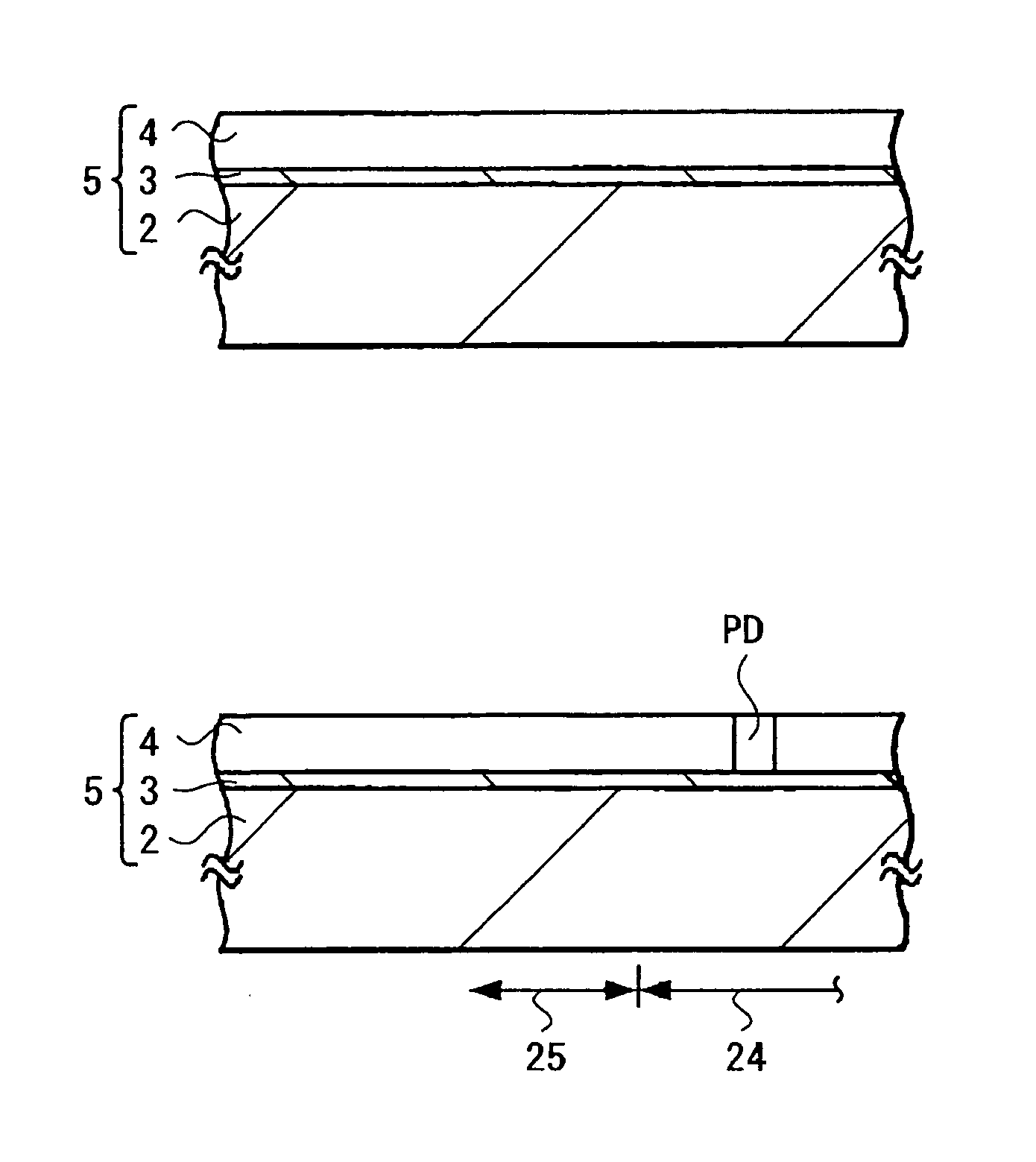
[0065]FIG. 2 is a schematic diagram (cross-sectional view) of a CMOS type solid-state image pickup device, and FIG. 3 is a cross-sectional view showing a main portion of FIG. 2 in an enlarged-scale. A color filter and an on-chip microlens are not shown in FIG. 2.

[0066] As shown in FIGS. 2 and 3, in a CMOS type solid-state image pickup device 10 according to the embodiment of the present invention, an image pickup region 24 includes a single crystal silicon layer (semiconductor substrate) 4 in which unit pixels 22, each of which is composed of a photoelectric conversion element (photodiode PD) and a plurality of MOS type transistors Tr1, are arranged in ...


PUM


Abstract

A method of manufacturing a solid-state image pickup device comprises a process for forming a plurality of photoelectric conversion elements PD within a semiconductor substrate 4, a process for forming an interconnection portion, having an interconnection layer 8 in an insulating layer 7, on the surface side of the semiconductor substrate 4, a process for forming an adhesive layer, made of a material cured at a temperature lower than a deterioration starting temperature of the interconnection layer 8, on the surface of the interconnection portion and bonding a supporting substrate 30 to the surface side of the interconnection portion through the adhesive layer 9 by heat treatment at a temperature lower than the deterioration starting temperature of the interconnection layer 8 and a process for decreasing a thickness of the semiconductor substrate 4 from the back side. A solid-state image pickup device manufacturing method can bond the supporting substrate 30 to the surface side of the interconnection portion through the adhesive layer 9 without exerting a thermal influence upon the interconnection layer 8 that was previously formed on the surface side of the semiconductor substrate 4.

Description

BACKGROUND OF THE INVENTION [0001] 1. Field of the Invention [0002] The present invention relates to a solid-state image pickup device and a manufacturing method thereof and a semiconductor integrated circuit device and a manufacturing method thereof. [0003] 2. Description of the Related Art [0004] A related-art solid-state image pickup device includes a semiconductor substrate in which circuit elements, interconnection layers and the like are formed on the surface side thereof and in which photodiodes and the like are formed on the back side thereof to introduce light from the surface side of the semiconductor substrate to pick up an image. [0005] However, in the case of such arrangement, incident light is absorbed or reflected on the circuit elements, the interconnection layers and the like formed on the surface side of the semiconductor substrate so that efficiency at which incident light is photoelectrically converted is low, sensitivity of the solid-state image pickup device be...

Claims


Application Information

Patent Timeline
Patent Type & Authority Applications(United States)
IPC IPC(8): H01L27/14H01L21/00H01L21/31H01L21/469H01L27/146
CPCH01L27/14627H01L27/14636H01L27/14683H01L27/14643H01L27/14638H01L27/14
Inventor MURAMATSU, MASAFUMI
Owner SONY CORP
Why Eureka
Try Eureka