Monolithic silicon-based phased arrays for communications and radars

a phased array and silicon-based technology, applied in the field of wireless communications, can solve the problems of system waste, increased interference, and increased effects of multi-path fading and interferen

Active Publication Date: 2005-10-13
CALIFORNIA INST OF TECH
View PDF17 Cites 27 Cited by
  • Summary
  • Abstract
  • Description
  • Claims
  • Application Information

AI Technical Summary

Benefits of technology

[0022] In accordance with the present invention, an N-element phased-array receiver includes, in part, N RF mixers, and a signal summing block. Each RF mixer is adapted to receive a pair of input signals. The first signal applied to each RF mixer is an RF signal received by a receive antenna associated with that RF mixer. Accordingly, there are N receive antennas each associated with a different one of the N RF mixers. The second signal applied to each RF mixer is a local oscillator (LO) phase signal selected from among M phases of the local oscillator. Each of N phase selectors—each phase selector being associated with a different one of the N RF mixers—receives the M different phases of the local oscillator independently and, in response to one or more control signals, selects and supplies one of the M phases to its associated RF mixer. Therefore, the second signal applied to each RF mixer is a phase signal sup

Problems solved by technology

Such systems, however, have a number of drawbacks.
For example, the transmitter in such systems radiates electromagnetic power in all directions, only a small fraction of which reaches the intended receiver; this results in a considerable amount of waste in the transmitted power.
Furthermore, because the electromagnetic propagation is carried out in all directions, the effects of phenomenon such as multi-path fading and interference are more

Method used


Image

  • Monolithic silicon-based phased arrays for communications and radars
  • Monolithic silicon-based phased arrays for communications and radars
  • Monolithic silicon-based phased arrays for communications and radars

Examples


Embodiment Construction

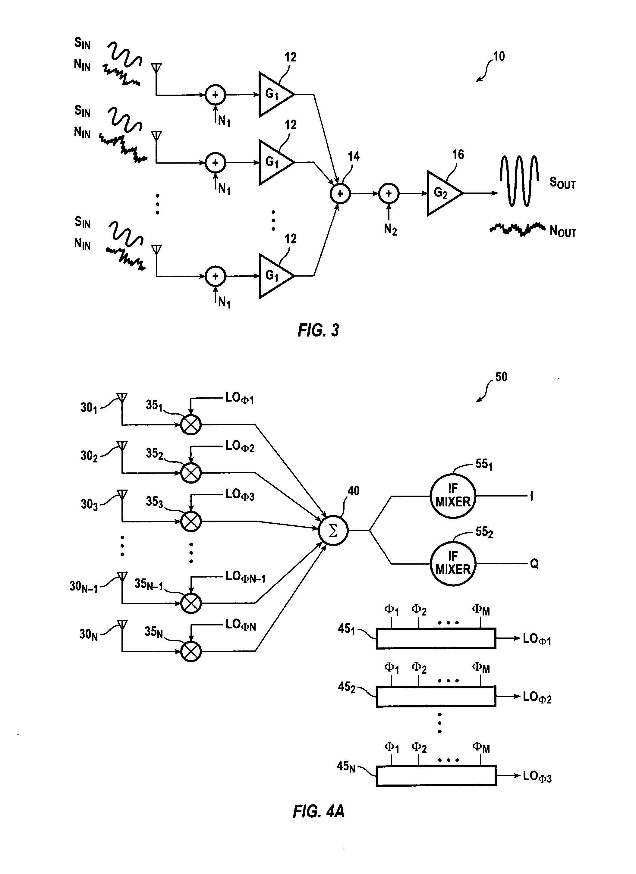
[0053] In accordance with one embodiment of the present invention, an N-element phased-array receiver, such as phased-array receiver 50 shown in FIG. 4A, includes, in part, N RF mixers 351, 352, 353 . . . 35N-1, 35N, and a signal summing block 40. Each RF mixer 35i, where i is an integer ranging from 1 to N, is adapted to receive a pair of input signals. The first signal applied to each RF mixer 35i is an RF signal received by a receive antenna 30i associated with that RF mixer 35i. Accordingly, there are N receive antennas 30i each associated with a different one of the N RF mixers 35i. The second signal applied to each RF mixer 35 is a phase signal LOΦi selected from among M phases Φ1, Φ2 . . . ΦM of a local oscillator. Each of N phase selectors 451, 452, 453 . . . 45N-1, 45N—each phase selector being associated with a different one of the N RF mixers 35i—receives the M different phases Φ1, Φ2, . . . ΦM of the local oscillator independently and, in response to one or more control ...


PUM


Abstract

A phased-array receiver is adapted so as to be fully integrated and fabricated on a single silicon substrate. The phased-array receiver is operative to receive a 24 GHz signal and may be adapted to include 8-elements formed in a SiGe BiCMOS technology. The phased-array receiver utilizes a heterodyne topology, and the signal combining is performed at an IF of 4.8 GHz. The phase-shifting with 4 bits of resolution is realized at the LO port of the first down-conversion mixer. A ring LC VCO generates 16 different phases of the LO. An integrated 19.2 GHz frequency synthesizer locks the VCO frequency to a 75 MHz external reference. Each signal path achieves a gain of 43 dB, a noise figure of 7.4 dB, and an IIP3 of −11 dBm. The 8-path array achieves an array gain of 61 dB, a peak-to-null ratio of 20 dB, and improves the signal-to-noise ratio at the output by 9 dB.

Description

CROSS-REFERENCES TO RELATED APPLICATIONS [0001] The present application claims benefit under 35 USC 119(e) of the filing date of U.S. provisional application No. 60 / 519,715, filed on Nov. 13, 2003, entitled “Monolithic Silicon-Based Phased Arrays for Communications and RADARS”, the content of which is incorporated herein by reference in its entirety.BACKGROUND OF THE INVENTION [0002] The present invention relates to wireless communications, and in particular to a phased-array receiver adapted for use in wireless communication systems. [0003] Omni-directional communication systems have been used extensively in various applications due, in part, to their insensitivity to orientation and location. Such systems, however, have a number of drawbacks. For example, the transmitter in such systems radiates electromagnetic power in all directions, only a small fraction of which reaches the intended receiver; this results in a considerable amount of waste in the transmitted power. Thus, for a ...

Claims


Application Information

Patent Timeline
IPC IPC(8): H01QH01Q3/22H01Q3/26H01Q3/42H01Q21/00H04B1/06H04B1/26H04B7/00
CPCH01Q3/22H01Q3/26H01Q21/0093H01Q3/42H01Q3/2682
Inventor HASHEMI, HOSSEINGUAN, XIANGHAJIMIRI, SEYED ALI
Owner CALIFORNIA INST OF TECH
Why Eureka
Try Eureka