Method of manufacturing optical crystal element of laser

Inactive Publication Date: 2005-10-20
SHIMADZU CORP
View PDF1 Cites 7 Cited by
  • Summary
  • Abstract
  • Description
  • Claims
  • Application Information

AI Technical Summary

Benefits of technology

[0018] After etching for a sufficiently short period of time in the practical sense, it is possible to obtain the optical crystal having a desired thickness and accurate tolerance.
[0019] According to the present invention, in the method of manufacturing an optical crystal element for a laser, it is possible to manufacture an optical crystal having a thickness of 1 mm or less

Problems solved by technology

Accordingly, it is difficult to reduce an overall size of the device.
Also, the device tends to have a complex configuration, thereby increasing cost.
In the conventional method, it is difficult to achieve thickness accuracy for an optical crystal of a microchip laser.

Method used


Image

  • Method of manufacturing optical crystal element of laser
  • Method of manufacturing optical crystal element of laser
  • Method of manufacturing optical crystal element of laser

Examples


Example

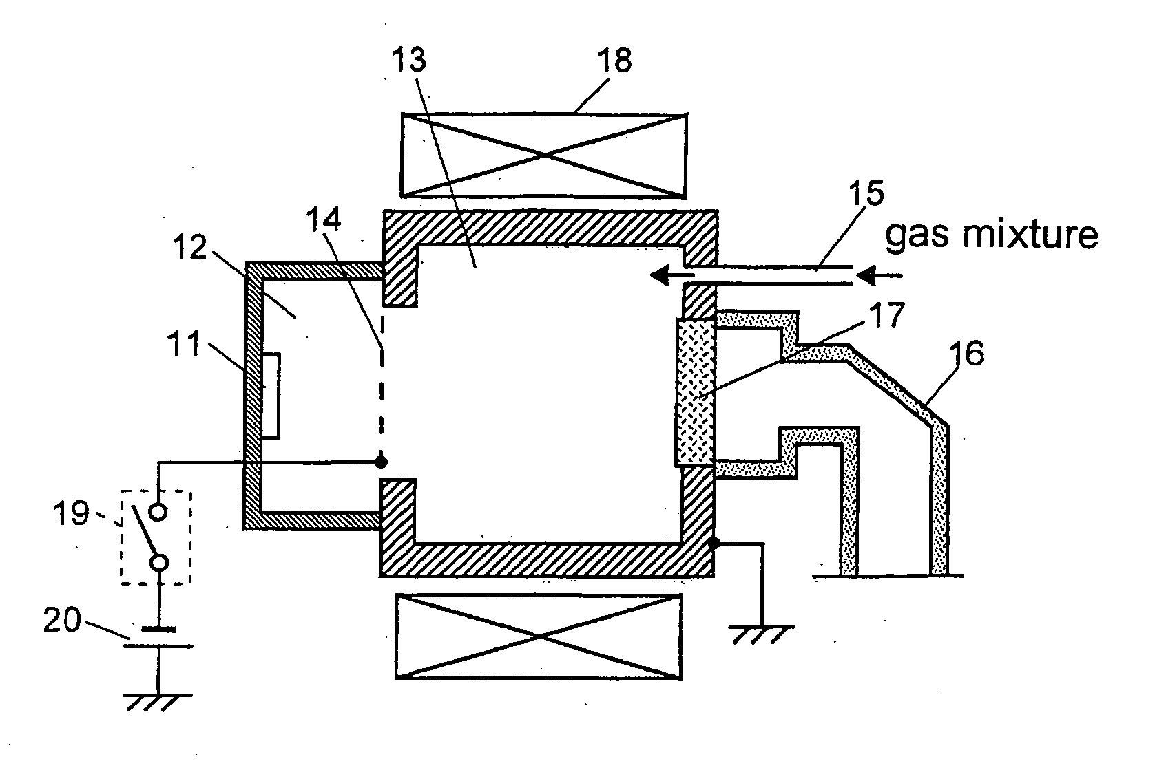
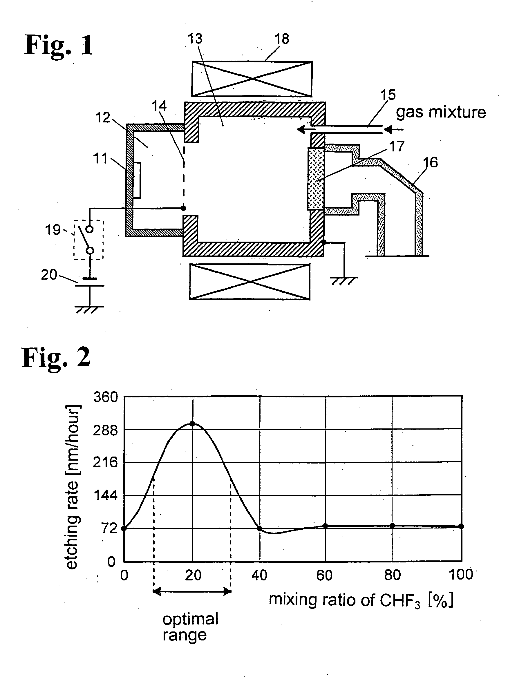
[0025] Hereunder, embodiments of the present invention will be explained with reference to the accompanying drawings. As an embodiment of the present invention, a method of manufacturing an optical crystal element formed of YAG for a microchip laser will be explained.

(i) Preparation of a Crystal Substrate and Measurement of Initial and Target Thicknesses

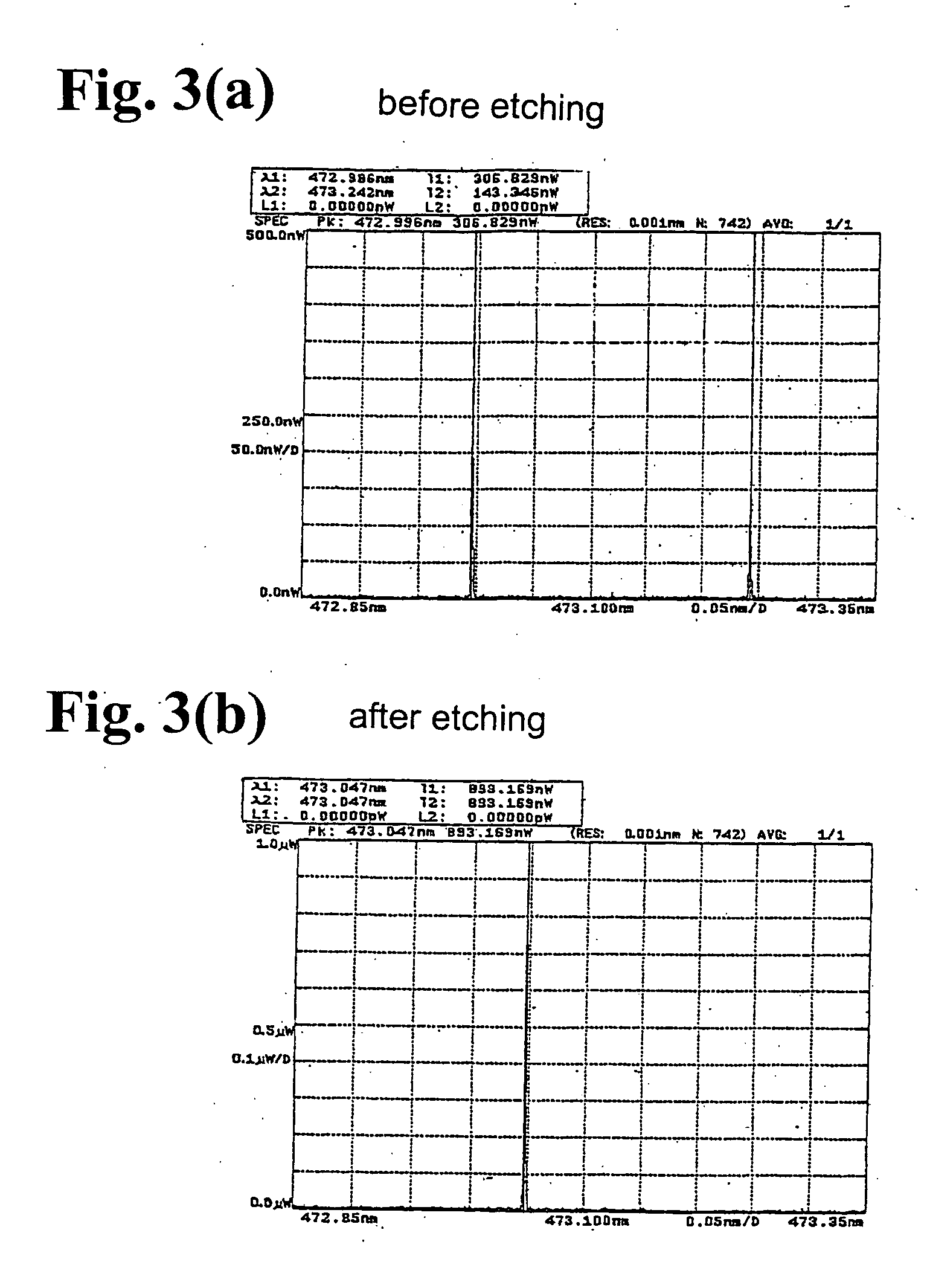
[0026] A surface of a YAG crystal was polished first to prepare a disk-shaped crystal substrate with a thickness d1=0.5 mm and a diameter of 20 mm. An initial thickness of the crystal substrate was measured. Various methods may be used to measure the initial thickness of the YAG crystal, and the thickness was measured with a tolerance of 10 nm using a spectroscope as described below.

[0027] In general, a crystal thickness d is given by the following formula:

m·λ=2·n·d·cosθ  (1)

where λ is a transmission wavelength of the crystal, m is an order of interference, n is a refractive index, and θ is an incident angle of laser. The crys...


PUM

PropertyMeasurementUnit
Thicknessaaaaaaaaaa

Abstract

A method of manufacturing an optical crystal element of a laser device includes measuring an initial thickness of a crystal substrate formed of YAG or YVO4; introducing a mixture of a fluorine gas and an Ar gas having a ratio of the fluorine gas to the Ar gas in a range of 1:10 to 1:2 into a process chamber holding the crystal substrate; and generating ion beams of the mixture in the process chamber for etching a surface of the crystal substrate for a period time determined from an etching rate depending on the ratio of the mixture and the initial thickness of the crystal substrate. Thickness of the optical crystal element is controlled to a desired thickness. In the method, it is possible to produce the optical crystal element of a microchip laser having functions as a laser medium, a resonator and an etalon.

Description

BACKGROUND OF THE INVENTION AND RELATED ART STATEMENT [0001] The present invention relates to a method of manufacturing an optical crystal element used in a semiconductor laser (LD) excitation solid-state laser device, and more specifically, relates to a method of manufacturing an optical crystal element having functions as a laser medium, resonator, and etalon, in a microchip laser. [0002] In recent years, a short wavelength laser such as a green laser and blue laser has been focused in a broad range of fields including an interferometer, an optical disc pick-up, and a printer device. Accordingly, research and development for laser devices generating such laser light has been actively pursued. In a known short wavelength laser device, a wavelength conversion element is inserted in a path of fundamental wave laser light for generating high-order harmonic wave laser light to be emitted outwardly. FIG. 4 is a schematic view showing a structure of the laser device. [0003] The laser dev...

Claims


Application Information

Patent Timeline
IPC IPC(8): H01S3/06C30B29/28C30B29/30C30B33/12H01S3/094H01S3/14
CPCC30B29/28C30B33/12C30B29/30
Inventor TATENO, RYO
Owner SHIMADZU CORP
Why Eureka
Try Eureka