
Single scan irradiation for crystallization of thin films

a single-scan irradiation and crystallization technology, applied in the field of single-scan irradiation for crystallization of thin films, can solve the problems of low throughput rate, and achieve the effect of improving the crystalline properties of polycrystalline films and a simple and time-efficient process

Inactive Publication Date: 2005-10-27
THE TRUSTEES OF COLUMBIA UNIV IN THE CITY OF NEW YORK
View PDF99 Cites 55 Cited by
  • Summary
  • Abstract
  • Description
  • Claims
  • Application Information

AI Technical Summary

Benefits of technology

[0018] In one aspect, the method avoids the need to scan the same area of the substrate multiple times in order to fully crystallize the film. It also provides a simpler and time-efficient process that translates the system in the x- and y-directions during laser irradiation. Furthermore, it provides grains that are elongated beyond their characteristic lateral growth length, thereby further improving the crystalline properties of the polycrystalline film.

Problems solved by technology

Although the resultant polycrystalline films have elongated grains with enhanced mobilities, the many iterative steps of irradiation and translation result in low throughput rates.

Method used


Image

  • Single scan irradiation for crystallization of thin films
  • Single scan irradiation for crystallization of thin films
  • Single scan irradiation for crystallization of thin films

Examples


Embodiment Construction

[0036] Sequential lateral solidification is a particularly useful lateral crystallization technique because it is capable of grain boundary location-controlled crystallization and provides crystal grains of exceptionally large size. Sequential lateral solidification produces large grained structures through small-scale translation of a thin film between sequential pulses emitted by a pulsed laser. As the film absorbs the energy of each pulse, a small area of the film melts completely and recrystallizes laterally from the solidus / melt interface to form a crystalline region. By “lateral crystal growth” or “lateral crystallization,” as those terms are used herein, it is meant a growth technique in which a region of a film is melted to the film / surface interface and in which recrystallization occurs in a crystallization front moving laterally across the substrate surface. “Characteristic lateral growth length,” as that term is used herein, means the length of unimpeded lateral growth of...


PUM

PropertyMeasurementUnit
angleaaaaaaaaaa
δaaaaaaaaaa
angle thetaaaaaaaaaaa

Abstract

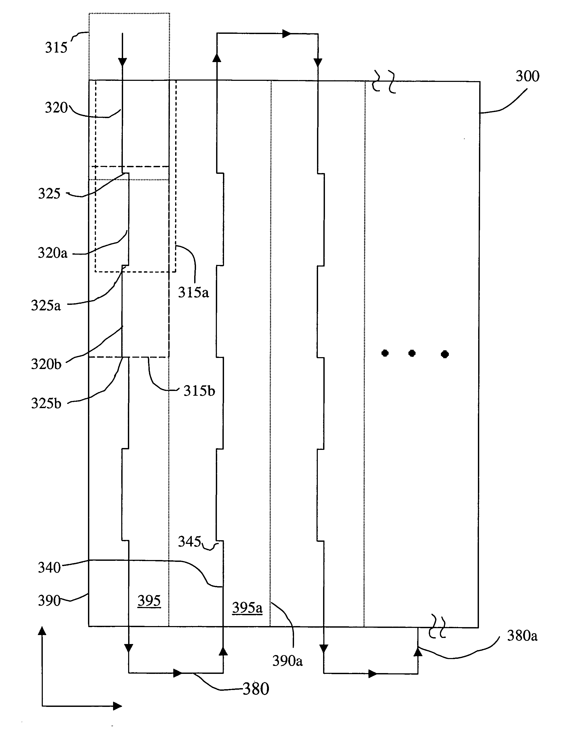
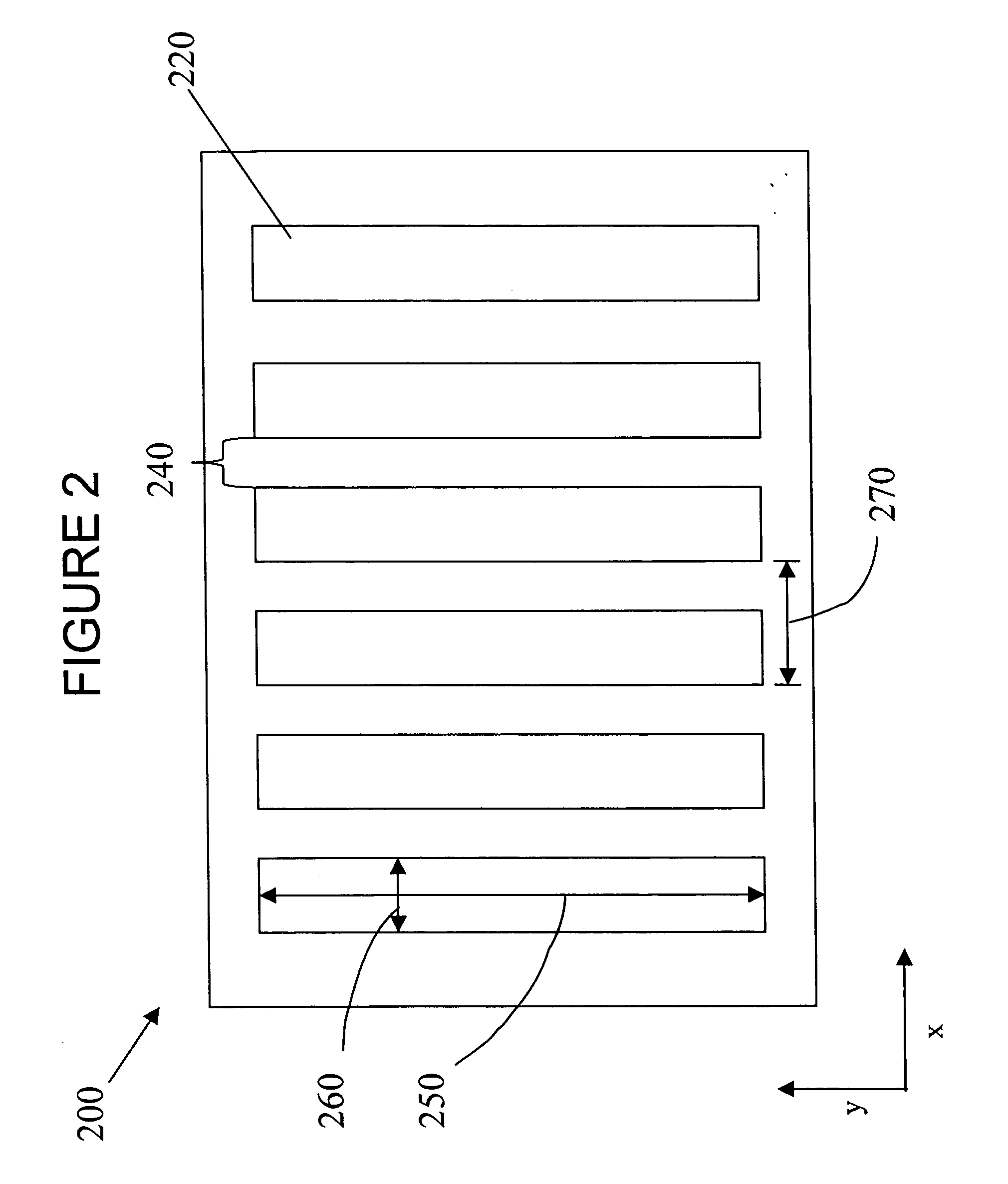
A method of processing a polycrystalline film on a substrate includes generating a plurality of laser beam pulses, positioning the film on a support capable of movement in at least one direction, directing the plurality of laser beam pulses through a mask to generate patterned laser beams; each of said beams having a length l′, a width w′ and a spacing between adjacent beams d′, irradiating a region of the film with the patterned beams, said beams having an intensity that is sufficient to melt an irradiated portion of the film to induce crystallization of the irradiated portion of the film, wherein the film region is irradiated n times; and after irradiation of each film portion, translating either the film or the mask, or both, a distance in the x- and y-directions, where the distance of translation in the y-direction is in the range of about 1′ / n-δ, where δ is a value selected to form overlapping the beamlets from the one irradiation step to the next, and where the distance of translation in the x-direction is selected such that the film is moved a distance of about λ′ after n irradiations, where λ′=w′+d′.

Description

RELATED APPLICATIONS [0001] This application claims priority under 35 U.S.C. § 119(e) to co-pending U.S. Application Ser. No. 60 / 504,270, filed Sep. 19, 2003, and entitled “Single Scan Irradiation for Crystallization of Thin Films,” the contents of which are incorporated herein by reference.FIELD OF THE INVENTION [0002] This invention relates to methods and systems for processing thin film material, and more particularly to forming large-grained, grain-boundary-location controlled thin films from amorphous or polycrystalline thin films using laser irradiation. In particular the present invention relates to methods and systems for the production of integrated thin film transistors. BACKGROUND OF THE INVENTION [0003] In recent years, various techniques for crystallizing or improving the crystallinity of an amorphous or polycrystalline semiconductor film have been investigated. This technology is used in the manufacture of a variety of devices, such as image sensors and active-matrix l...

Claims


Application Information

Patent Timeline
Patent Type & Authority Applications(United States)
IPC IPC(8): C30B1/00C30B3/00C30B5/00C30B13/24G03F7/20H01L
CPCB23K26/0656C30B13/24C30B28/08C30B35/00Y10T117/10G03F7/70725Y10S117/90Y10T117/1008G03F7/70041B23K26/066
Inventor IM, JAMES S.VAN DER WILT, PAUL CHRISTIAN
Owner THE TRUSTEES OF COLUMBIA UNIV IN THE CITY OF NEW YORK
Learn More