Solid-state image sensing element and its design support method, and image sensing device

a technology of image sensing element and design support method, which is applied in the direction of radioation control device, television system, instruments, etc., can solve the problems of light rays not being able to enter the photoelectric conversion unit, phenomenon posing severe bottlenecks, and frame periphery often becoming dark, so as to improve the degree of design freedom and high light collecting efficiency

Active Publication Date: 2005-10-27
CANON KK
View PDF28 Cites 139 Cited by
  • Summary
  • Abstract
  • Description
  • Claims
  • Application Information

AI Technical Summary

Benefits of technology

[0031] The present invention has been made in consideration of the above situation, and has as its first object to provide a solid-state image sensing element which can imp

Problems solved by technology

However, when the condition of the exit pupil of the image sensing lens changes, light rays cannot enter the photoelectric conversion unit and the frame periphery often becomes dark.
Especially, when an image sensing lens that has a zoom function and focus adjustment function is used, the phenomenon poses severe bottlenecks.
However, boosting a signal level to an appropriate level by applying electrical gain is to enhance not only signal components but also noise components, resulting in a low-quality image in which noise is conspicuous on the darkening-corrected peripheral portion.
In case of the conventional compact digital camera, the type of its image sensing sys

Method used


Image

  • Solid-state image sensing element and its design support method, and image sensing device
  • Solid-state image sensing element and its design support method, and image sensing device
  • Solid-state image sensing element and its design support method, and image sensing device

Examples


first embodiment

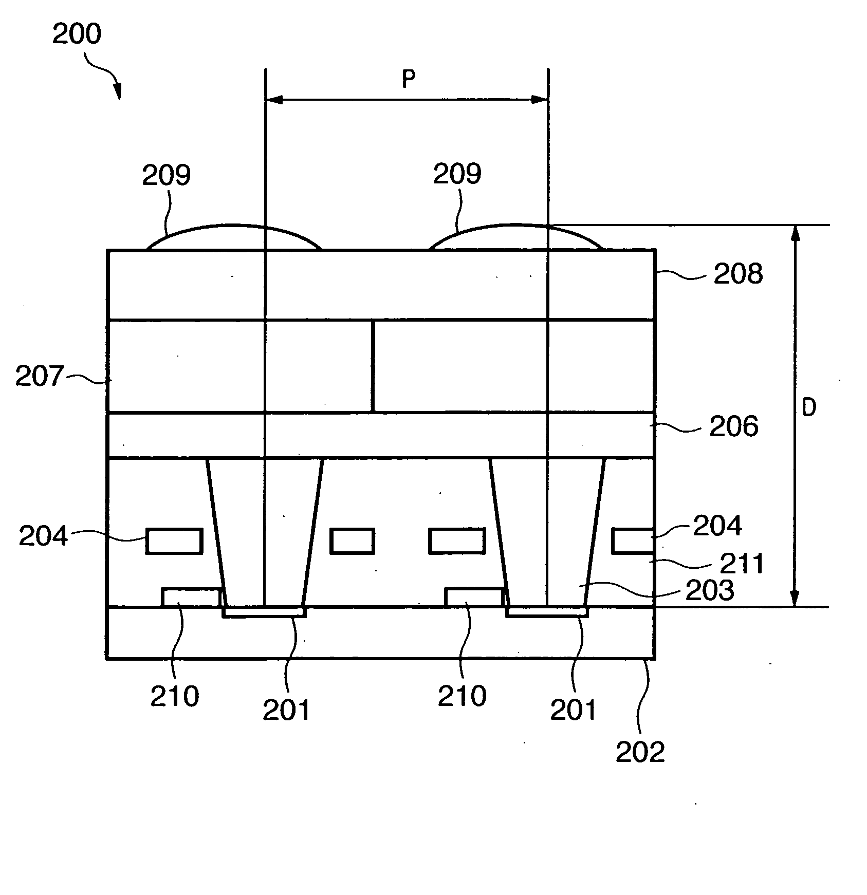
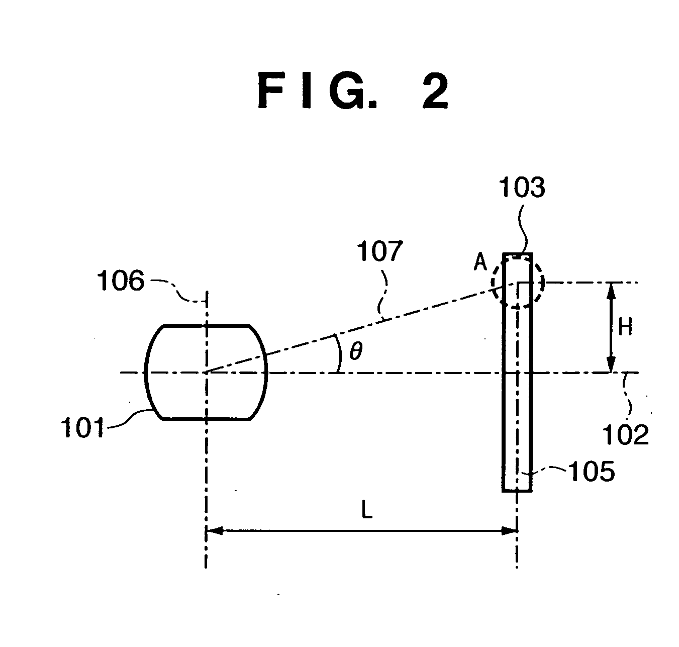
[0076]FIG. 1 is a sectional view showing the concept of the arrangement of an image sensing device such as a digital still camera system and the like. Referring to FIG. 1, reference numeral 101 denotes a convex lens as an imaging optical system; 102, an optical axis of the imaging optical system 101; 103, an image sensor for converting an object light image formed by the imaging optical system into an electrical signal; and 104, a housing that holds the imaging optical system 101 and image sensor 103, and has a function as a camera obscura. Note that the imaging optical system 101 is illustrated as a single lens (convex lens) for the descriptive convenience. In practice, the imaging optical system can be an imaging optical system having positive power by combining a plurality of lenses, reflecting mirrors, or diffraction imaging optical systems. Also, a zoom function may be applied. Furthermore, the imaging optical system 101 may have a stop for light shielding that cuts ghost and f...

second embodiment

[0139]FIG. 14 is a side sectional view showing a schematic structure of a digital color camera as an image sensing device according to the second embodiment of the present invention. This camera is a single-plate type digital color camera using an image sensing element such as a CCD, CMOS sensor, or the like, and obtains an image signal indicating a moving or still image by driving the image sensing element continuously or in a one-shot manner. Note that the image sensing element is an area sensor which converts incoming light into charges according to the amount of light, accumulates the charges for respective pixels, and reads out the accumulated charges.

[0140] Referring to FIG. 14, reference numeral 110 denotes a camera body; and 126, a lens device which includes an image sensing lens 125 and is detachable from the camera body 110. Note that FIG. 14 depicts only one lens as the image sensing lens 125. However, the image sensing lens 125 is normally formed by combining a pluralit...

third embodiment

[0206] The light guide can be formed by combining other materials.

[0207] In the third embodiment, in the color image sensing element with the structure shown in FIG. 23, the insulating interlayer 38 is formed of silicon oxide (SiO2) and the embedded transparent layer 36 is formed of silicon nitride (Si3N4) unlike in the second embodiment.

[0208] Since the refractive index of the embedded transparent layer 36 is 2.0 and that of silicon oxide (SiO2) that forms the insulating interlayer 38 that neighbors the embedded transparent layer 36 (silicon nitride) is 1.46, a refractive index difference of about 1.37 times is generated. For this reason, light rays that obliquely enter the boundary surface beyond the critical angle from the high refractive index side toward the low refractive index side can be totally reflected. With such light guide structure, obliquely coming light is efficiently guided to the photoelectric conversion unit 31.

[0209] Furthermore, in the third embodiment, the f...


PUM


Abstract

A solid-state image sensing element has a photoelectric conversion element which converts incoming light into an electrical signal in accordance with an amount of the light, a microlens which is arranged on an incident surface, a light guide which is arranged between the photoelectric conversion element and the microlens, and an insulating interlayer which is arranged around the light guide. The solid-state image sensing element located at a distance (H) satisfies: H·DL·P<a·NHNLfor0<a<1
where L is the distance from an exit pupil of an image sensing optical system of an image sensing device, which mounts an image sensor formed by two-dimensionally arranging a plurality of the solid-state image sensing elements, H is the distance from a center of the image sensor to a position of the solid-state image sensing element on the image sensor, D is the height from the photoelectric conversion element to an apex of the microlens, P is the spacing between the plurality of solid-state image sensing elements, NH is the refractive index of the light guide, and NL is the refractive index of the insulating interlayer.

Description

FIELD OF THE INVENTION [0001] The present invention relates to an image sensing device having a zoom function and focus adjustment function in an image sensing optical system, a lens-exchangeable image sensing device, a solid-state image sensing element used in the image sensing device and its design support method, and a device. BACKGROUND OF THE INVENTION [0002] In recent years, solid-state image sensing elements mainly used in digital still cameras and the like are roughly classified into a CCD (Charge-Coupled Device) and CMOS (Complementary Metal Oxide Semiconductor) (e.g., see Japanese Patent Laid-Open Nos. 2002-141488 and 2002-083948). [0003] Principal components of the structure of the CCD will be briefly explained first with reference to FIG. 28. [0004]FIG. 28 is a sectional view of one pixel of a CCD 1000. Referring to FIG. 28, reference numeral 1001 denotes a semiconductor substrate formed of, e.g., silicon; 1002, a photoelectric conversion element including a photodiode; ...

Claims


Application Information

Patent Timeline
IPC IPC(8): G02B3/00G02B6/00H01L21/82H01L27/00H01L27/146H01L31/0216H01L31/0232
CPCH01L27/14621H01L27/14625H01L27/14627H01L27/14629H01L31/02162H01L31/0232H04N2101/00H01L27/14685H01L31/02327
Inventor NOTO, GOROSUDA, YASUONAGANO, AKIHIKO
Owner CANON KK
Why Eureka
Try Eureka