Image sensor and offset-able reference voltage generator thereof

a reference voltage generator and image sensor technology, applied in the field of offset compensation circuits, can solve the problems of increasing the required chip area, consuming the most power in the process of generating analog reference voltage, and fixed pattern noise on the display screen, so as to reduce the number of operational amplifiers deployed inside the image sensor, save the chip area, and reduce the production cost

Inactive Publication Date: 2005-10-27
SUNPLUS TECH CO LTD
View PDF2 Cites 32 Cited by
  • Summary
  • Abstract
  • Description
  • Claims
  • Application Information

AI Technical Summary

Benefits of technology

[0009] Accordingly, the present invention is directed to an image sensor capable of correcting (compensating an offset voltage) the reference voltage of a pixel sampling circuit first and hence eliminating the offset-correction circuit inside various sample/hold circuits. Hence, some chip area is saved thereby lowering production cost. Furthermore, beca

Problems solved by technology

In the image sensor read-out circuit, the process of generating analog reference voltage consumes the most power.
On the other hand, factors such as production offset, circuit loading and layout area of sampling capacitor often lead to a fixed pattern noise on the display screen between vertical columns.
In other words, the require

Method used


Image

  • Image sensor and offset-able reference voltage generator thereof
  • Image sensor and offset-able reference voltage generator thereof
  • Image sensor and offset-able reference voltage generator thereof

Examples


Embodiment Construction

[0026] Reference will now be made in detail to the present preferred embodiments of the invention, examples of which are illustrated in the accompanying drawings. Wherever possible, the same reference numbers are used in the drawings and the description to refer to the same or like parts.

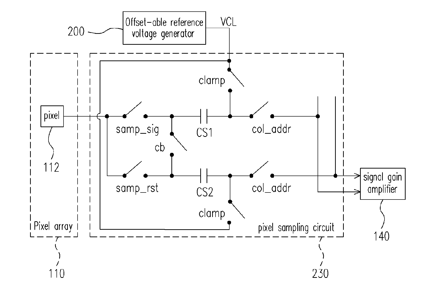
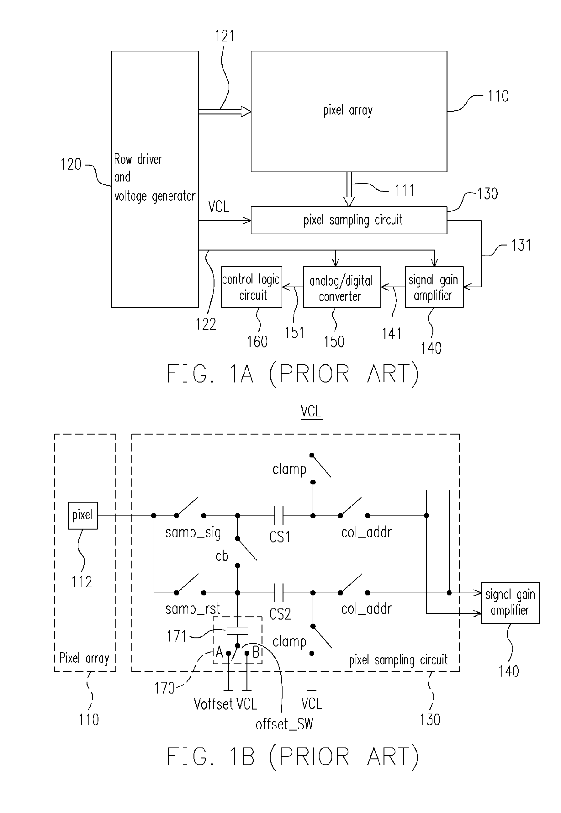
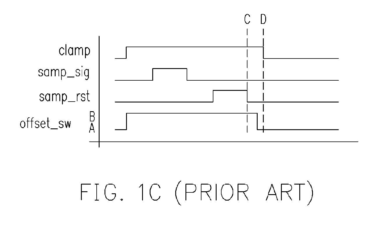
[0027] To simplify the following descriptions, a CMOS image sensor is used as an example. In the conventional technique, the sample / hold circuits in each column of pixels must have a corresponding set of offset-correcting circuits. However, as the number of pixels in an image sensor grow larger and larger, more and more offset-correcting circuits (each one comprising at least an offset-compensating capacitor and an operational amplifier) are required. Furthermore, the operational amplifiers for driving the offset-compensating capacitors also consume a lot of power. Hence, overall power consumption of the operation amplifiers is increased as the number of columns in a pixel array rises. Moreover, du...


PUM


Abstract

An image sensor and offset-able reference voltage generator thereof are provided. The image sensor comprises a plurality of pixels, an offset-able reference voltage generator and a pixel sampling circuit. The pixel senses light from an image and generate an image signal. The offset-able reference voltage generator provides a reference voltage having a voltage offset. The pixel sampling circuit is coupled to the pixels and the offset-able reference voltage generator to sample the image signal and generate a pixel signal according to the reference voltage. The voltage offset of the reference voltage is able to compensate for the offset voltage in the process of generating the pixel signals.

Description

CROSS-REFERENCE TO RELATED APPLICATION [0001] This application claims the priority benefit of Taiwan application serial no. 93111372, filed Apr. 23, 2004. BACKGROUND OF THE INVENTION [0002] 1. Field of the Invention [0003] The present invention relates to an offset compensation circuit. More particularly, the present invention relates to an image sensor and offset-able reference voltage generator. [0004] 2. Description of Related Art [0005] In recent years, more and more electronic products such as mobile phones, personal digital assistant and toys incorporate a built-in camera. To meet various personal requirements, especially portability of the mobile devices, image sensors with low power consumption and high picture quality are in great demand. FIG. 1A is a block diagram of a conventional image sensor. As shown in FIG. 1A, the image sensor comprises an array of pixels 110, a row driver / voltage generator 120, a sample and hold circuit 130, a signal gain amplifier 140 and an analog...

Claims


Application Information

Patent Timeline
IPC IPC(8): H01L31/00H04N5/217
CPCH04N5/3575H04N5/378H04N5/365H04N25/616H04N25/67H04N25/75
Inventor BLERKOM, DANIEL VANCHEN, I-SHIOU
Owner SUNPLUS TECH CO LTD
Why Eureka
Try Eureka