Scanning probe microscope and specimen surface structure measuring method

Inactive Publication Date: 2005-11-03
RIKEN
View PDF7 Cites 32 Cited by
  • Summary
  • Abstract
  • Description
  • Claims
  • Application Information

AI Technical Summary

Benefits of technology

[0009] As can be seen from equations (1) and (2), lowering the atomic force Fc by regulating it to a fixed quantity with the servo will prove effective in reducing the measurement position errors Δr and Δz. In other words, it is important that a small atomic force be used to control the system. The conventional art utilized the atomic force of the repulsive force region to accomplish this. However, the minimum atomic force is approximately 10−8N so achieving a measurement position error of 1 nanometer or less, requires setting an atomic force regulated to 10−10N or less.
[0018] The scanning probe microscope of the present invention may used for measurement of tiny devices or may be used to measure defects. This scanning probe microscope may also be used as a line monitor in the semiconductor manufacturing process. In the basic probe operation during measurement, when the scanning stops the surface position is measured, and during scanning the probe is separated from the specimen surface. The vibration method (non-contact) method is used simultaneous with probe operation at a force setting of 10−10N and below. Therefore, even with an aspect ratio of 10 or more, errors of 1 nanometer or less due to slip of the probe can be suppressed, and high precision shape measurement can be performed.

Problems solved by technology

However, the minimum atomic force is approximately 10−8N so achieving a measurement position error of 1 nanometer or less, requires setting an atomic force regulated to 10−10N or less.

Method used


Image

  • Scanning probe microscope and specimen surface structure measuring method
  • Scanning probe microscope and specimen surface structure measuring method
  • Scanning probe microscope and specimen surface structure measuring method

Examples


first embodiment

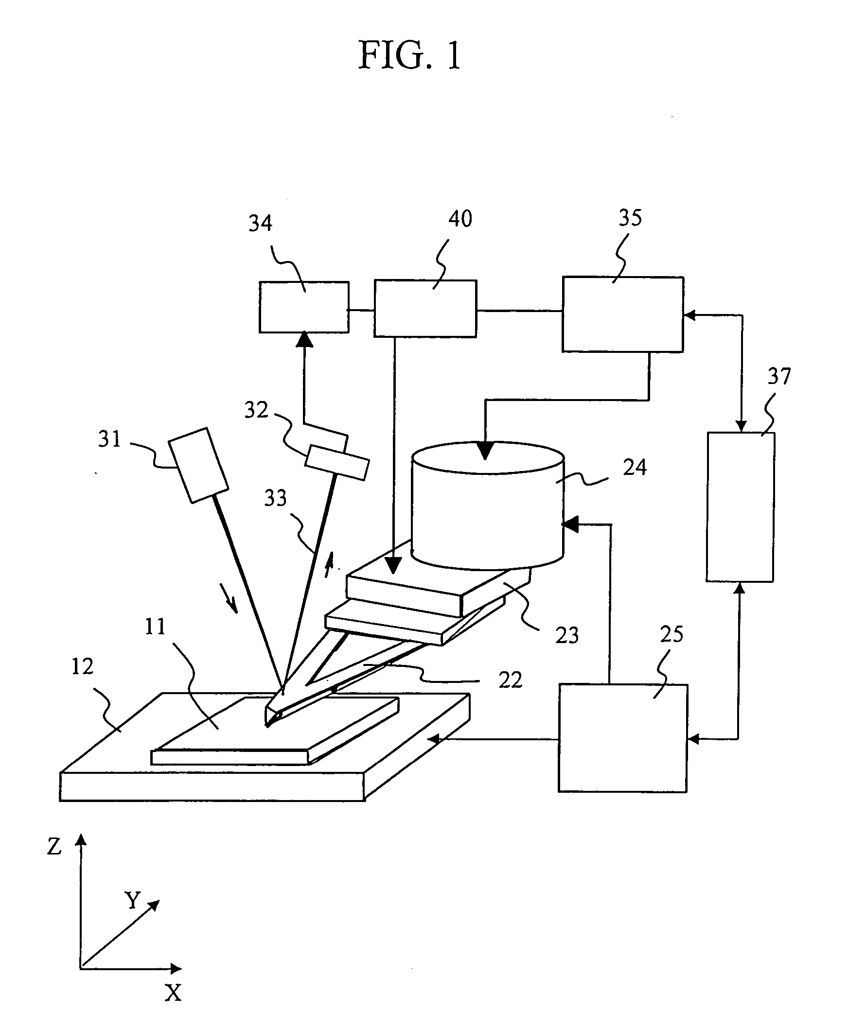
[0030]FIG. 1 is a block diagram showing an example of the digital probing AFM of the present invention using the slope detection method. In addition to the usual AFM structure, this digital probing AFM contains a vibration mechanism for detecting the atomic force gradient.

[0031] The specimen 11 is mounted on the XY specimen stage 12. The XY specimen stage 12 is moved coarsely by the XY scanning circuit 25 so that the measurement region is selected directly below the probe. The cantilever 22 with the probe is attached on an exciter piezoelectric element 23 and a cylindrical XYZ scanning piezoelectric element 24. A normal optical lever method made up of a semiconductor laser 31, a position detector 32, and a force detector 34 is utilized as the force detector. The servo circuit 35 drives the probe in the Z direction by means of the XYZ scanning piezoelectric element 24, and servo controls the force to a fixed value with the signal detected by force detector 34. The XY scanning circui...

second embodiment

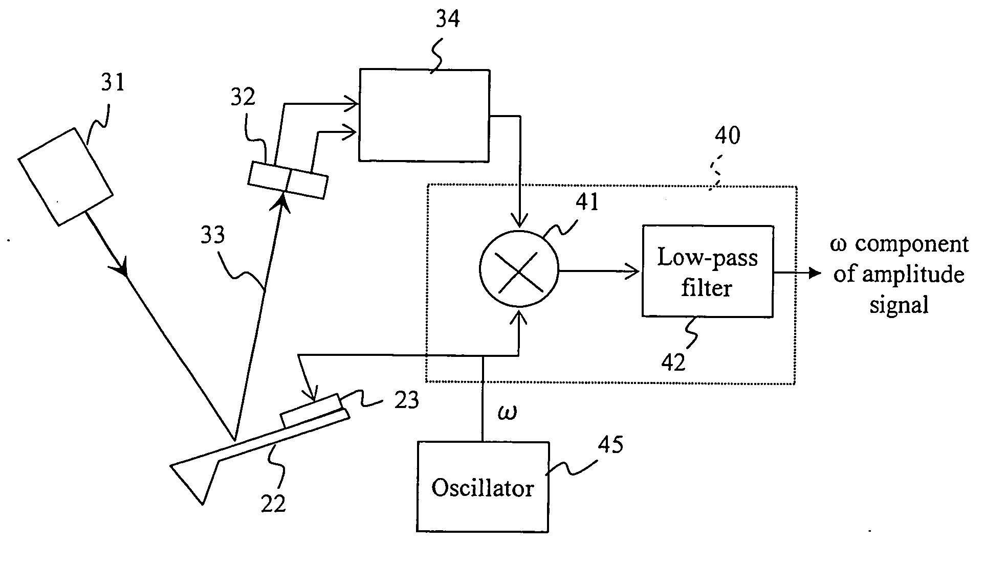
[0043]FIG. 6 is a concept block diagram of showing another example of digital probing AFM in the present invention. In addition to the usual AFM structure, this digital probing AFM contains an FM (frequency modulation) detection type atomic force gradient detector.

[0044] In the example in the drawing, the force detector utilizes an optical lever system made up of a semiconductor laser 31, a position detector 32, a force detector circuit 34. However in order to detect the force gradient, the frequency is demodulated using a PLL (phase-lock-loop) circuit 50 and the change in the force gradient detected from the change in the frequency. The servo system, scanning system, proximity mechanism, and probe position detector identical to the first embodiment are utilized to regulate the detected signal to a fixed value. Unlike the first embodiment, an external oscillator (or vibrator) is not used for self-vibrating the probe, instead a resonance circuit system in the internal circuit networ...

third embodiment

[0050]FIG. 9 is a concept block diagram of a semiconductor scanning device utilizing a digital probing AFM incorporating the slope detection method. The semiconductor scanning device shown in the figure contains an AFM having a function using the vibration method for detecting the atomic force gradient. This device further contains a chip position detection function for measuring at an optional measurement position within the semiconductor chip, as well as a computer processing function for automatic measurements.

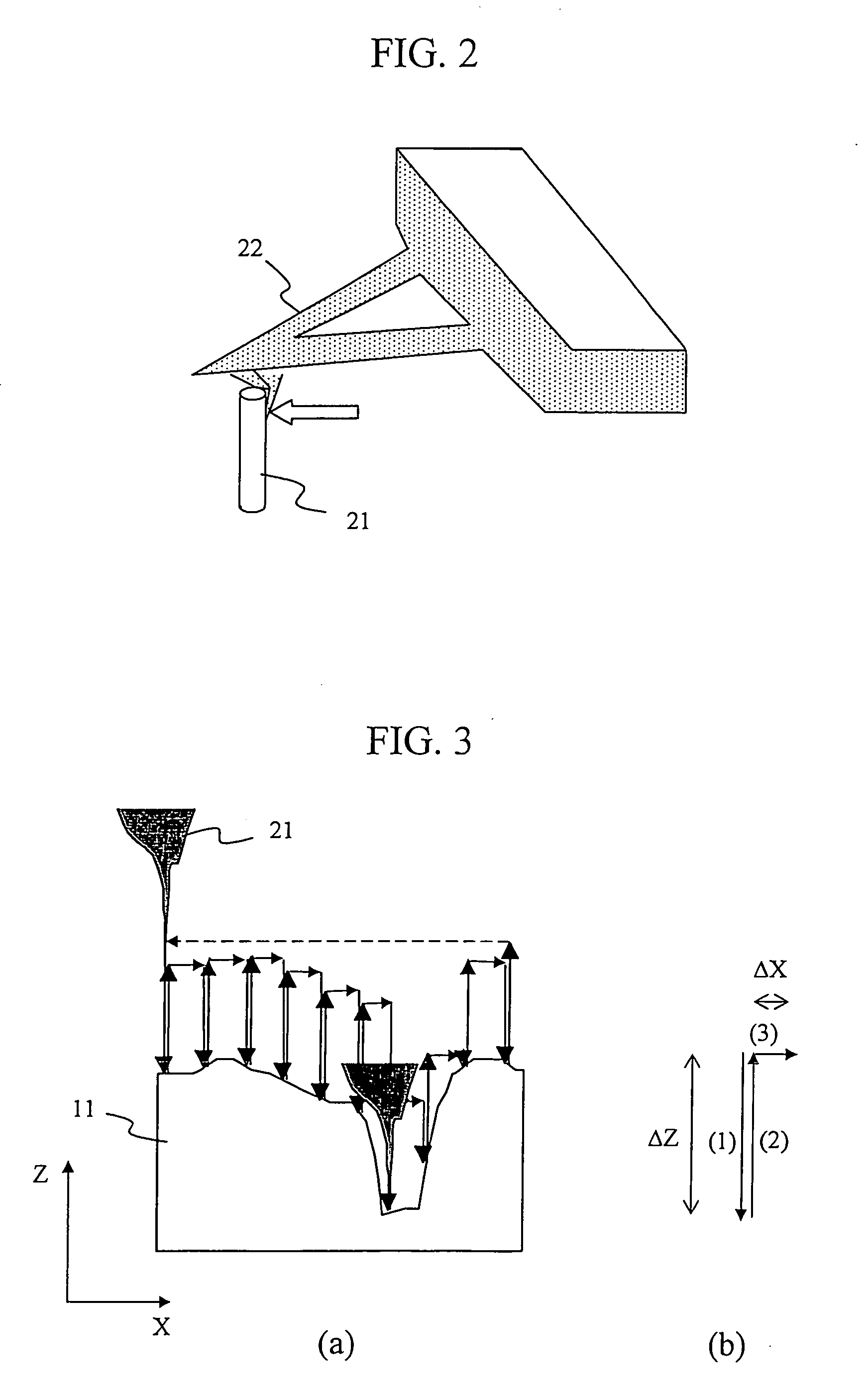
[0051] The force detector for the AFM utilizes the optical lever method. This force detector is made up of a semiconductor laser 31, a position detector 32, and a force detector 34. A lock-in amplifier 40 detects the force gradient the same as in the first embodiment. An approach device (not shown in drawing) is installed to make the probe 21 approach the surface of the specimen 11 (semiconductor chip).

[0052] In addition to the AFM measurement means, this embodiment furth...


PUM


Abstract

A digital probing type atomic force microscope (AFM) for measuring high aspect structures with high precision. A probe 21 is vibrated while moved to the vicinity of an atomic force region on a specimen surface. The position of the probe is measured when a specified atomic force is detected in the atomic force region. The probe is then moved away from the specimen surface. A servo system for maintaining a gap between the probe and specimen surface is stopped. The probe is moved to a measurement point along the specimen surface while kept away from the specimen. The vibration frequency is a frequency slightly offset from the cantilever resonance point. The atomic force is detected based on the vibration amplitude of the cantilever.

Description

TECHNICAL FIELD [0001] The present invention relates to a scanning probe microscope capable of making three-dimensional measurements on the nanometer order of accuracy on the surface structure of a specimen, and relates in particular to a probe microscope capable of accurate measurements of a surface structure with a fine structure on the nanometer level, and further possessing a high aspect ratio. BACKGROUND ART [0002] In recent years, along with the growth of our information society, there are increasing needs for technology capable of joint use of large amounts of information. The semiconductor field is making progress in miniaturization. Current leading edge technology is seeking to miniaturize devices to a minimum scale of 0.13 μm. Along with this progress, there is also a need for higher precision and greater miniaturization in device isolation technology, wiring technology and contact technology, etc. Structures with a higher aspect ratio (depth / aperture diameter) are also be...

Claims


Application Information

Patent Timeline
IPC IPC(8): G01B21/30G01Q10/04G01Q10/06G01Q20/02G01Q60/24G01Q60/32G01Q60/38G01Q70/12
CPCB82Y15/00B82Y35/00G01Q70/12G01Q30/04G01Q60/34G01Q10/06
Inventor HASEGAWA, TSUYOSHIAONO, MASAKAZUNAKAYAMA, TOMONOBUHOSAKA, SUMIO
Owner RIKEN
Why Eureka
Try Eureka