Method for manufacturing semiconductor device

a semiconductor and manufacturing technology, applied in the direction of identification means, instruments, optics, etc., to achieve the effect of reducing the influence of electric property differences

Inactive Publication Date: 2005-11-03
SEMICON ENERGY LAB CO LTD
View PDF66 Cites 7 Cited by
  • Summary
  • Abstract
  • Description
  • Claims
  • Application Information

AI Technical Summary

Benefits of technology

[0009] In view of the foregoing status of the art, it is an object of the present invention to provide a method for manufacturing a semiconductor device which restrains the influence of difference in electric property between circuits requiring consistency of plural TFTs as in the above-described current mirror circuit.

Problems solved by technology

As a result, if the electrical properties of the two transistors are not equal, I1=I2 cannot necessarily be achieved and therefore the current mirror circuit does not function as a circuit.

Method used


Image

  • Method for manufacturing semiconductor device
  • Method for manufacturing semiconductor device
  • Method for manufacturing semiconductor device

Examples


embodiment mode 1

[0055] An embodiment mode of the present invention will now be described with reference to FIGS. 3 to 5. FIGS. 3 to 5 show a method for preparing a semiconductor device according to the present invention. In FIGS. 3A and 3B and FIGS. 4A and 4B, oblique views are shown on the left side and top views are shown on the right side. FIGS. 5A to 5F simply show the method for preparing a semiconductor device according to the present invention.

[0056] A semiconductor 102 is formed on a substrate 101 (FIG. 3A). As the substrate 101, any material that is durable to the processing temperature throughout the manufacture of a semiconductor device may be used. For example, a quartz substrate, a silicon substrate, a non-alkaline glass substrate containing barium borosilicate glass or aluminoborosilicate glass or the like, or a substrate having an insulating film formed on a surface of a metal substrate can be used. Also a plastic substrate that is heat-resistant enough to be durable to the processi...

embodiment mode 2

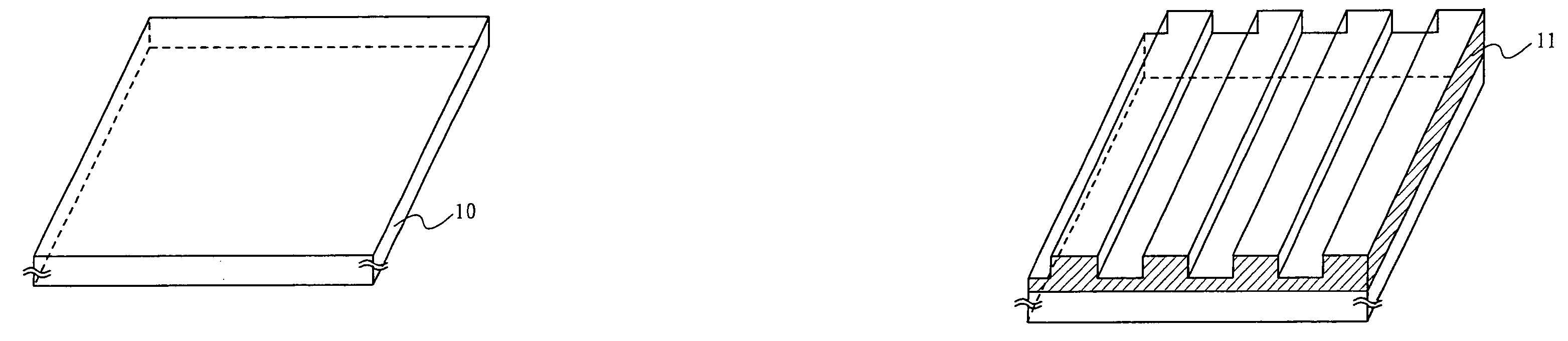
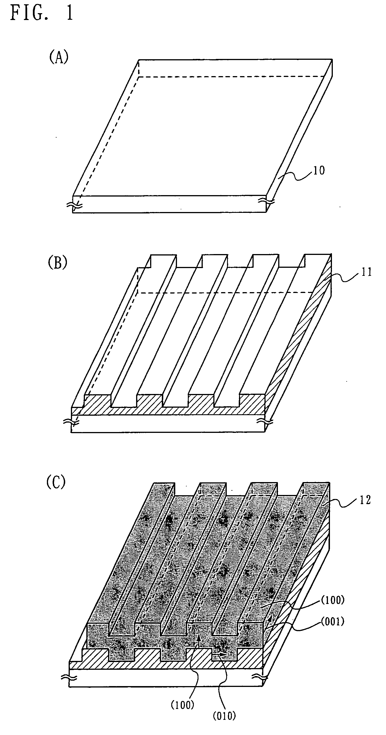
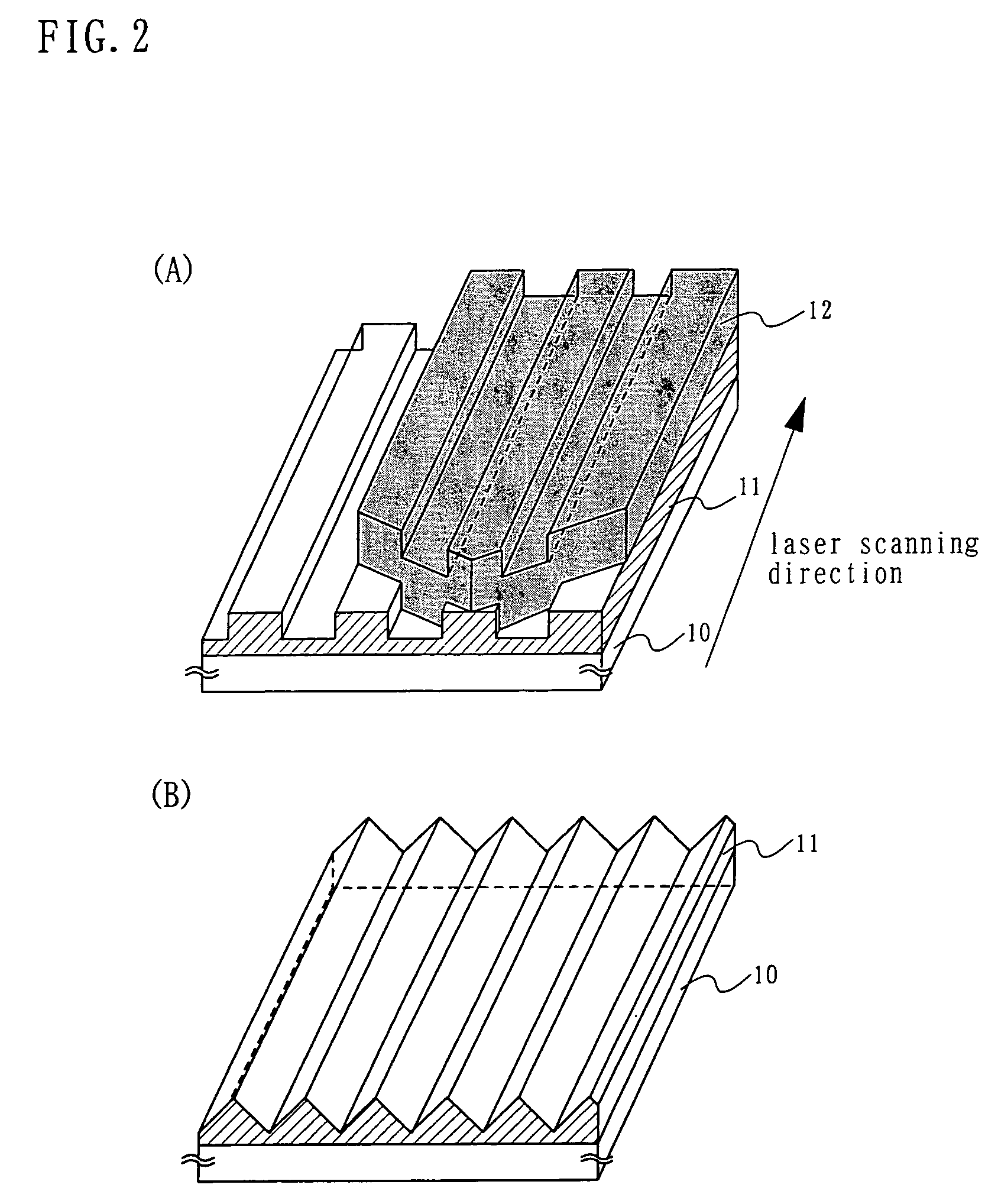
[0075] In this embodiment mode, as a different embodiment mode from Embodiment Mode 1, a method for preparing a semiconductor device to which the principle of grapho-epitaxy is applied will be described with reference to FIGS. 1 and 2.

[0076] The basic principle of grapho-epitaxy utilizes the anisotropy of surface energy held by crystals to be grown. The anisotropy of surface energy means a characteristic such that, for example, crystals of salt grown from a solution exhibit regular hexahedrons. In the case of an SOI structure, it means the anisotropy of surface energy between SiO2 and Si.

[0077] In FIG. 1A, 10 represents a substrate. As the substrate 10, any material that is durable to the processing temperature throughout the manufacture of a semiconductor device may be used. For example, a quartz substrate, a silicon substrate, a non-alkaline glass substrate containing barium borosilicate glass or aluminoborosilicate glass or the like, or a substrate having an insulating film for...

embodiment mode 3

[0090] In this embodiment mode, top views in the case where a gate electrode and source and drain wirings are formed on an island-like semiconductor layer formed by using the methods for preparing a semiconductor device described in Embodiment Modes 1 and 2 will be described with reference to FIGS. 6 to 9.

[0091] In FIG. 6, 1 represents a first island-like semiconductor layer, and 2 and 4 represent a source wiring and a drain wiring, respectively or vice versa. 3 represents a gate electrode and 5 represents a contact hole. FIGS. 6A to 6C represent second island-like semiconductor layers.

[0092] In FIG. 4A, three second island-like semiconductor layers 105 are formed from a first island-like semiconductor layer 104. In this specification, the three first island-like semiconductor layers, from the side close to a-point, are referred to as second island-like semiconductor layer 6A, second island-like semiconductor layer 6B, and second island-like semiconductor layer 6C. In the present ...


PUM

PropertyMeasurementUnit
wavelengthaaaaaaaaaa
deflection angleaaaaaaaaaa
diameteraaaaaaaaaa

Abstract

A method for manufacturing a semiconductor device having steps of forming an amorphous semiconductor on a substrate having an insulating surface; patterning the amorphous semiconductor to form plural first island-like semiconductors; irradiating a linearly condensed laser beam on the plural first island-like semiconductors while relatively scanning the substrate, thus crystallizing the plural first island-like semiconductors; patterning the plural first island-like semiconductors that have been crystallized to form plural second island-like semiconductors; forming plural transistors using the plural second island-like semiconductors; and forming a unit circuit using a predetermined number of the transistors, where the second island-like semiconductors used for the predetermined number of the transistors are formed from the first island-like semiconductors that are different from each other.

Description

[0001] This invention relates to a semiconductor device and a method for preparing the same. DESCRIPTION OF THE RELATED ART [0002] Recently, a technique has been broadly used in which an amorphous semiconductor layer formed on an insulating material such as a glass substrate is crystallized to provide a crystalline semiconductor layer and a thin film transistor (hereinafter referred to as TFT) using the crystalline semiconductor layer as an active layer is formed. Its electrical property has been significantly improved. [0003] As a result, a signal processing circuit, which was externally mounted using an IC or the like in the conventional technique, can be formed using a TFT, and a display device in which a pixel part and a driving circuit are integrally formed on a substrate is realized. Since the small size and light weight of the display device because of reduction in number of components enable significant reduction in manufacturing cost, a broad range of research and developme...

Claims


Application Information

Patent Timeline
Patent Type & Authority Applications(United States)
IPC IPC(8): G02F1/1368G09F9/00H01L21/20H01L21/268H01L21/336H01L21/77H01L21/84H01L27/12H01L29/423H01L29/49H01L29/786
CPCH01L21/2026H01L27/12H01L29/42384H01L29/4908H01L29/66757H01L27/1285H01L29/78603H01L29/78621H01L29/78675H01L27/1281H01L29/66765H01L21/02683H01L21/02488H01L21/02422H01L21/02496H01L21/0242H01L21/02609H01L21/02672H01L21/02425H01L21/02686H01L21/02678H01L21/02532H01L21/02381H01L21/02691
Inventor AZAMI, MUNEHIROKOKUBO, CHIHOSHIGA, AIKOISOBE, ATSUOSHIBATA, HIROSHIYAMAZAKI, SHUNPEI
Owner SEMICON ENERGY LAB CO LTD
Why Eureka
Try Eureka