Epitaxial structure of gallium nitrIde series semiconductor device and process of manufacturing the same

a gallium nitride and semiconductor technology, applied in the field of epitaxial structure of gallium nitride semiconductor devices and the same manufacturing process, can solve the problems of reducing illumination efficiency, affecting the performance of illumination devices, and inevitably generating crystal structures, so as to increase the performance and service life of semiconductor devices, and reduce the defect density

Inactive Publication Date: 2005-11-10
SEMILEDS OPTOELECTRONICS CO LTD
View PDF8 Cites 15 Cited by
  • Summary
  • Abstract
  • Description
  • Claims
  • Application Information

AI Technical Summary

Benefits of technology

[0009] It is therefore an object of the invention to provide an epitaxial structure of a gallium nitride series semiconductor and a process of manufacturing the same. A first buffer layer made of gallium nitride is epitaxially grown over a substrate at a first temperature. A second buffer layer made of indium gallium nitride is formed on the first buffer layer at a second temperature. The second temperature is then increased to a third temperature. While the temperature is increasing, precursors such as In(CH3)3 and NH3 are used for surface treatment of the second buffer layer. Thereafter, an epitaxial gallium nitride layer is grown at the third temperature. The structure of the obtained buffer layer and the process of growing such a buffer layer allow perfect crystal and low defect density, effectively increasing the performance and service life of a semiconductor device.

Problems solved by technology

In the case that the layers are epitaxially formed, defects are inevitably generated in their crystal structures.
Performance of the illumination devices is adversely affected thereby in several aspects such as, for example, reduced illumination efficiency, lowered electron shifting, and prolonged diffusion paths for dopants.
Moreover, V-shaped trenches, resulting in layer dislocation, appear in the quantum wells of active layers.
If cracks or gaps appear in the crystal structure, an illumination device cannot be grown above the cracks or gaps, because the illumination device formed on such an area has a short service life and low illumination efficiency.
Gallium nitride bulks are difficult to grow so that, currently, gallium nitride must be formed on a sapphire- or SiC-based substrate.
The gallium nitride layer directly formed on the substrate is not reliable and therefore a buffer layer must be formed between the substrate and the gallium nitride.
This kind of lateral epitaxial growth effectively reduces the defect density, but complicates the production of the mask.
Meanwhile, the elective growth mechanism increases the whole production cost.
However, the uniformity and the density of the SiN micromask are not easily controlled, and the yield is not easily controlled, either.

Method used


Image

  • Epitaxial structure of gallium nitrIde series semiconductor device and process of manufacturing the same
  • Epitaxial structure of gallium nitrIde series semiconductor device and process of manufacturing the same
  • Epitaxial structure of gallium nitrIde series semiconductor device and process of manufacturing the same

Examples


Embodiment Construction

[0019] Wherever possible in the following description, like reference numerals will refer to like elements and parts unless otherwise illustrated.

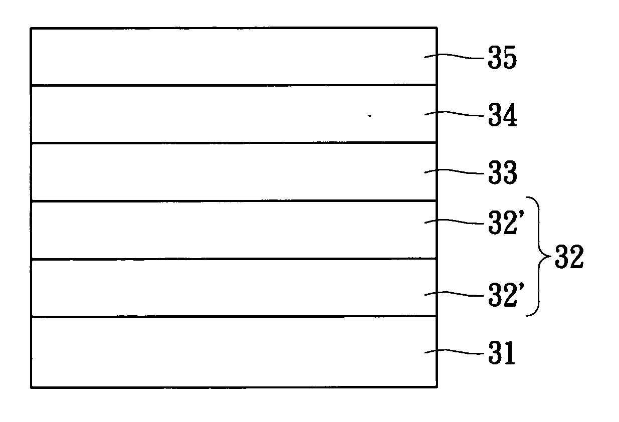
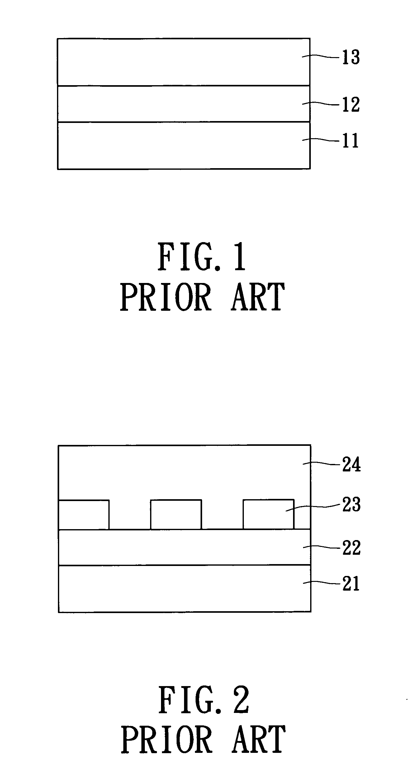
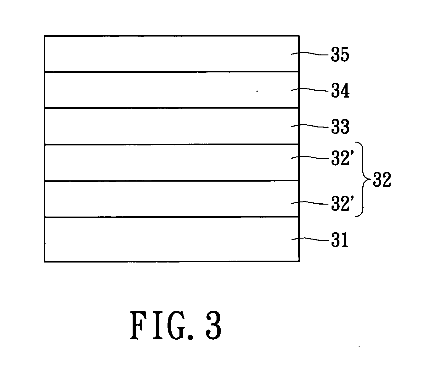
[0020] In one preferred embodiment of the invention, the invention provides an epitaxial structure of a gallium nitride series semiconductor device. Referring to FIG. 3, an epitaxial structure 30 includes a substrate 31, a first gallium nitride buffer layer 32, a second indium gallium nitride buffer layer 33 and an epitaxial gallium nitride layer 34. In the epitaxial structure 30, the substrate 31 is formed from sapphire, SiC, ZnO or Si. The first gallium nitride buffer layer 32 further includes, from bottom to top, a low-temperature gallium nitride buffer layer 32′ and a high-temperature gallium nitride buffer layer 32″. Furthermore, the epitaxial structure 30 further includes an epitaxy gallium nitride layer 35 on the epitaxial gallium nitride 34.

[0021]FIG. 4 is a flowchart illustrating the formation of the epitaxial structure according...


PUM

PropertyMeasurementUnit
thicknessaaaaaaaaaa
thicknessaaaaaaaaaa
temperatureaaaaaaaaaa

Abstract

An epitaxial structure of a gallium nitride series semiconductor device and a process of forming the same are described. A first buffer layer of gallium nitride is epitaxially formed on a substrate at a first temperature. A second buffer layer of indium gallium nitride is formed on the first buffer layer at a second temperature. The second temperature increases up to a third temperature, during which precursors including In(CH3)3 and NH3 are used for surface treatment. A high-temperature gallium nitride is formed at the third temperature. The buffer layer and the way to form such a buffer layer allow improved crystal configuration and lowered defect density, thereby increasing the performance and service life of a semiconductor device.

Description

BACKGROUND OF THE INVENTION [0001] 1. Field of the Invention [0002] The invention generally relates to an epitaxial structure of a gallium nitride semiconductor device and a process of manufacturing the same, and more particularly to a process of growing an epitaxial layer as a buffer layer. [0003] 2. Description of the Related Art [0004] Illumination devices can be formed of different layers. In the case that the layers are epitaxially formed, defects are inevitably generated in their crystal structures. Performance of the illumination devices is adversely affected thereby in several aspects such as, for example, reduced illumination efficiency, lowered electron shifting, and prolonged diffusion paths for dopants. Moreover, V-shaped trenches, resulting in layer dislocation, appear in the quantum wells of active layers. Furthermore, initial reverse bias is also increased. If cracks or gaps appear in the crystal structure, an illumination device cannot be grown above the cracks or ga...

Claims


Application Information

Patent Timeline
Patent Type & Authority Applications(United States)
IPC IPC(8): H01L21/20H01L21/205H01L29/20
CPCH01L21/0237H01L21/02458H01L29/2003H01L21/0254H01L21/02505
Inventor HON, SCHANG-JINGLAI, MU-JEN
Owner SEMILEDS OPTOELECTRONICS CO LTD
Why Eureka
Try Eureka