Method of manufacturing clad board for forming circuitry, clad board and core board for clad board

a manufacturing method and technology for forming circuits, applied in the direction of printing element electric connection formation, weaving, transportation and packaging, etc., can solve the problems of short circuit or lower insulating reliability between wiring, problems that increase at a higher density of wiring patterns, etc., to prevent short circuits, increase the yield rate of circuit boards, and prevent insulating reliability from lowering

Inactive Publication Date: 2005-11-10
PANASONIC CORP
View PDF15 Cites 2 Cited by
  • Summary
  • Abstract
  • Description
  • Claims
  • Application Information

AI Technical Summary

Benefits of technology

[0012] The present invention aims to prevent a short circuit due to a gap produced on an interface between a conventional pre-preg sheet and a releasing film. The present invention also aims to prevent insulating reliability from lowering, and increase a yield rate of circuit boards. The present invention aims to provide a clad board for forming circuitry, a method of manufacturing the clad boards, and a core board of the clad board.

Problems solved by technology

However, the method discussed above has the following problems.
As a result, a pattern touches an adjacent pattern while the circuits are formed, which produces a short-circuit or lowers insulating reliability between wiring.
These problems increases at a higher density of wiring patterns.

Method used


Image

  • Method of manufacturing clad board for forming circuitry, clad board and core board for clad board
  • Method of manufacturing clad board for forming circuitry, clad board and core board for clad board
  • Method of manufacturing clad board for forming circuitry, clad board and core board for clad board

Examples


exemplary embodiment 1

[0021] A first exemplary embodiment of the present invention will be described with reference to FIG. 1A to FIG. 4F. FIG. 4A to FIG. 4F are sectional views illustrating a method of manufacturing a clad board for forming circuitry in accordance with the first exemplary embodiment. The manufacturing method includes a releasing-film-sticking step, a hole-forming step, conductive-paste-filling step, peeling-off step, heat-and-pressure-applying step, and circuit-forming step.

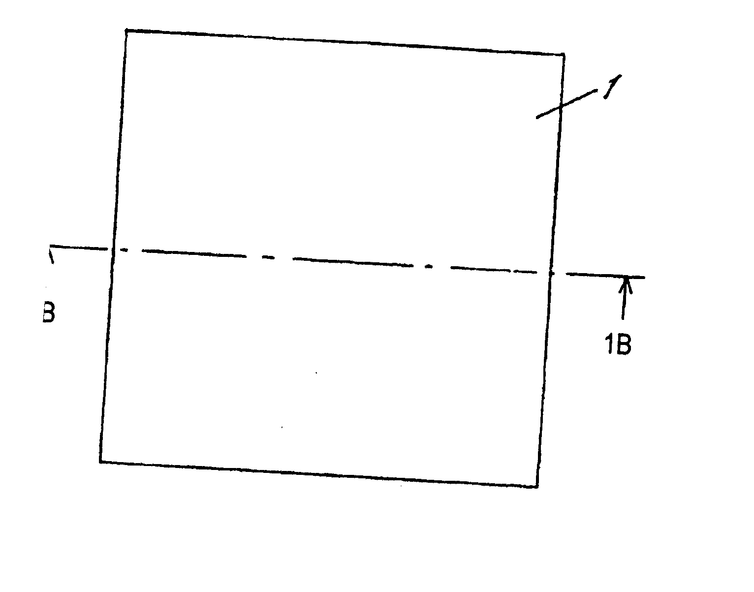
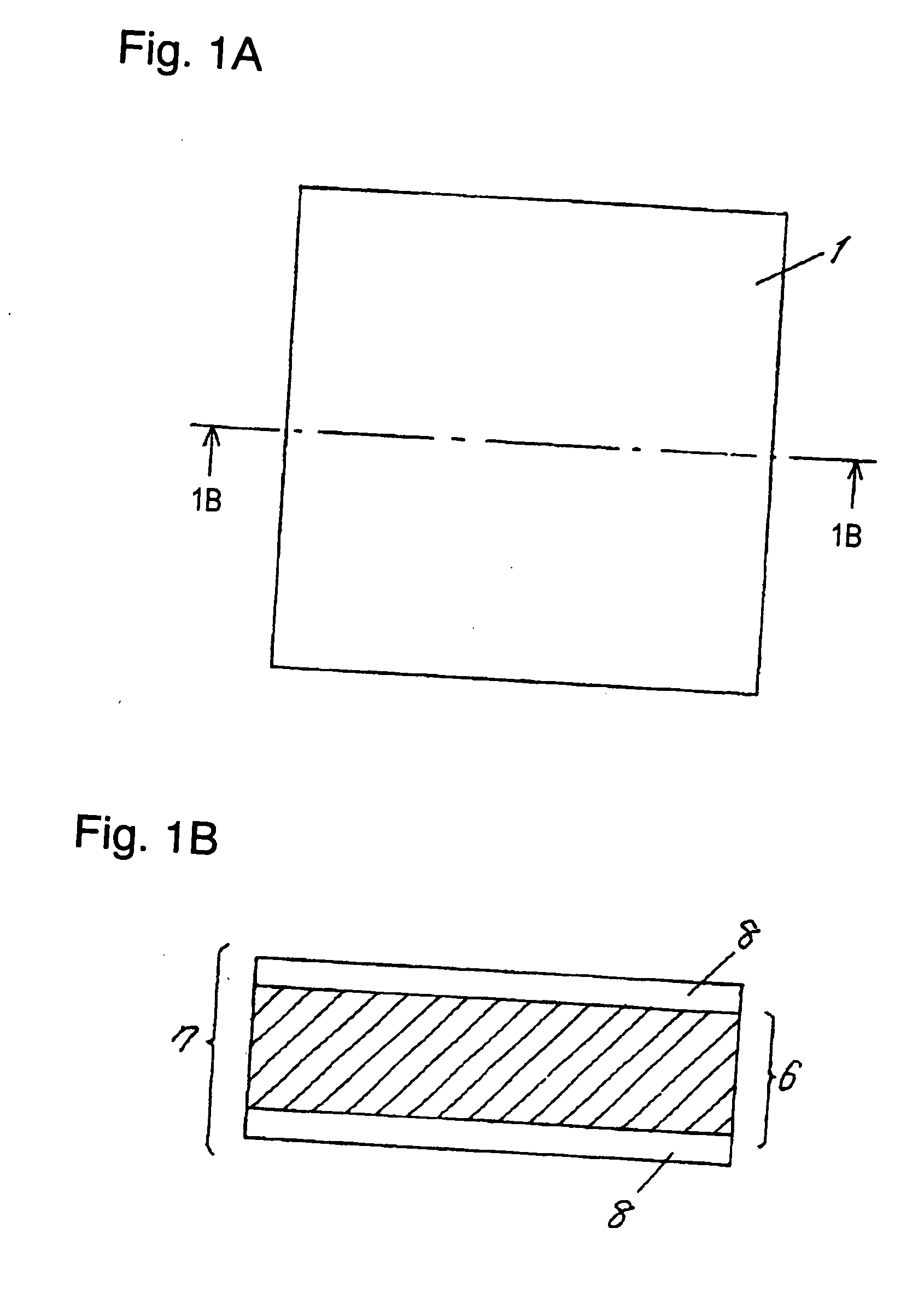
[0022] As shown in FIG. 1A and FIG. 1B, pre-preg sheet 1 is a composite material including impregnated resin 7 (e.g. thermosetting resin such as epoxy resin) and non-woven fabric 6 of fiber sheet such as aromatic polyamide fiber (aramid fiber). Impregnated resin 7 is not completely cured but includes a semi-cured portion, i.e., impregnated resin 7 is in B-stage.

[0023] Releasing film 2 shown in FIG. 4A is formed of polymer film such as polyethylene terephthalate (PET) of 20 μm thickness, having a silicon-based relea...

exemplary embodiment 2

[0036] A manufacturing method in accordance with a second exemplary embodiment is basically the same as that of the first embodiment, and detailed description is thus omitted here. Features only in the second embodiment will be described.

[0037] Pre-preg sheet 1 is a composite material formed of thermosetting resin such as epoxy resin (hereinafter called impregnated resin 7) and non-woven fabric 6 of fabric sheet such as aromatic polyamide fiber (aramid fiber). Impregnated resin 7 is not completely cured but includes semi-cured portions, i.e., impregnated resin 7 is in B-stage.

[0038] Aramid fiber non-woven fabric 6 conventionally used for pre-preg sheet 1 has a density ranging from 500 to 700 kg / m3. When resin is impregnated into such non-woven fabric 6, the center section of fabric 6 tends to be impregnated. Therefore, resin is not fully enough impregnated around a surface, and fibers of fabric 6 may be thus exposed on the surface in parts as shown in FIG. 6A and FIG. 6B.

[0039] H...

exemplary embodiment 3

[0047] A manufacturing method in accordance with a third exemplary embodiment is basically the same as that of the first embodiment, and detailed description is thus omitted here. Features only in the third embodiment will be demonstrated.

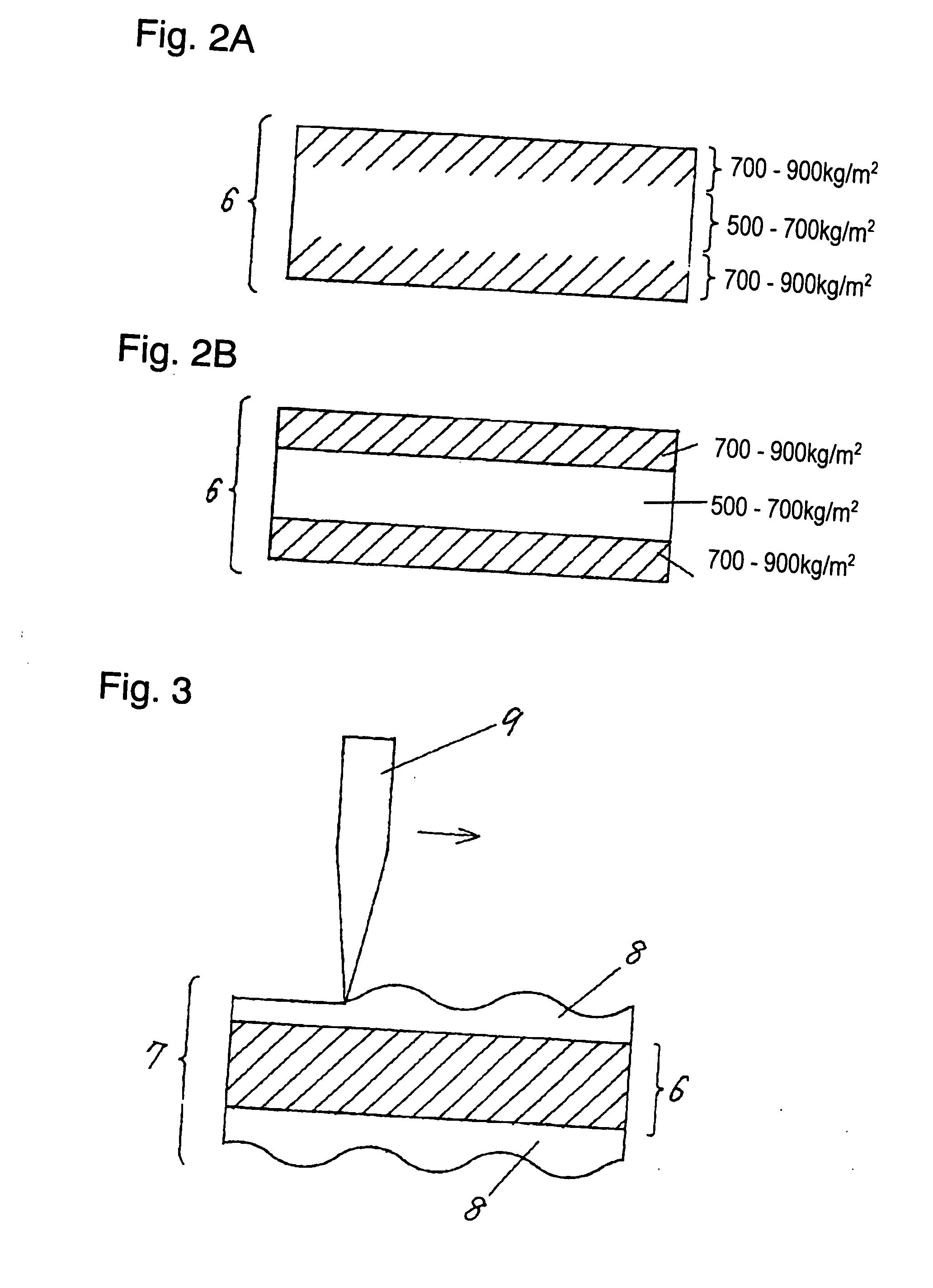
[0048] Aramid fiber non-woven fabric 6 used in the third embodiment has a density ranging from 700 to 1000 kg / m3 around a surface layer of both the faces of fabric 6 as shown in FIG. 2A. The density of the inside of fabric 6 is lower than that around the surface layer, and preferably ranges from 500 to 700 kg / m3.

[0049] If the density becomes lower than 500 kg / m3, a number of air-gaps in pre-preg sheet 1 increases. This makes conductive paste 4 tend to spread from inside of through holes 3 into pre-preg sheet 1 and the lowers its insulating reliability.

[0050] In pre-preg sheet 1 having the composition discussed above, resin is not impregnated well in the center section of aramid fiber non-woven fabric 6. Instead, much more resin component is atta...


PUM

PropertyMeasurementUnit
densityaaaaaaaaaa
thicknessaaaaaaaaaa
thicknessaaaaaaaaaa

Abstract

A manufacturing method of a clad board includes: sticking a releasing film to a pre-preg sheet; forming a non-through-hole or through-hole in the pre-preg sheet including the releasing film; filling the hole with conductive paste; peeling off the film; and heating and pressing a metal foil onto the pre-preg sheet. The clad board has a smooth face formed on one face or both the faces of the pre-preg sheet, so that the conductive paste is restrained from spreading in an interface between the pre-preg sheet and the releasing film. This structure can avoid short-circuit between circuits and prevent insulating reliability from lowering. As a result, an yield rate is improved, and a reliable circuit board is obtainable.

Description

TECHNICAL FIELD [0001] The present invention relates to a method of manufacturing a clad board for forming circuitry, the clad board, and a core board for the clad board. BACKGROUND ART [0002] Recently, electronic devices have been downsized, and components have been assembled at high densities into the devices. A conventional clad board for forming circuitry including electronics components mounted thereon has progressed from a single-sided board to a double-sided board, and a multi-layered board is now available. As such, a clad board to include the components at a higher density has been developed in order to accommodate more circuits therein. [0003] Instead of plated through-holes preventing a clad board from accommodating more circuits at a higher density, conductive paste for connections through inner via-holes is proposed (e.g. in Japanese Patent Application Laid-Open No.06-268345). [0004] In this method of manufacturing clad boards, a porous and compressive pre-impregnation ...

Claims


Application Information

Patent Timeline
Patent Type & Authority Applications(United States)
IPC IPC(8): H05K1/09B32B5/00B32B5/14B32B15/08H05K1/03H05K1/11H05K3/00H05K3/06H05K3/40
CPCB32B5/14B32B15/08H05K1/036H05K1/0366H05K3/4069H05K2201/0245Y10T428/2839H05K2203/0191H05K2203/1461Y10T428/24273Y10T428/24917Y10T29/49156H05K2201/0355Y10T428/249924Y10T428/24994Y10T428/249962Y10T428/249995Y10T442/2984Y10T442/607
Inventor YAMANE, SHIGERUKAWAMOTO, EIJIKOMODA, HIDEAKISUZUKI, TAKESHINISHII, TOSHIHIRONAKAMURA, SHINJI
Owner PANASONIC CORP
Why Eureka
Try Eureka