Method of inspecting pattern and inspecting instrument

a technology of pattern inspection and inspection instrument, which is applied in the direction of instruments, scanning probe techniques, semiconductor/solid-state device testing/measurement, etc., can solve the problems of failure of junction leakage location, and failure of junction leakage detection, etc., to achieve high accuracy, high yield, and high acceptability rate

Inactive Publication Date: 2005-11-10
HITACHI LTD
View PDF16 Cites 4 Cited by
  • Summary
  • Abstract
  • Description
  • Claims
  • Application Information

AI Technical Summary

Benefits of technology

[0013] Further, it is an object of the invention to provide a method and a system of inspection and a method of fabricating a semiconductor capable of optimizing a junction forming process and executing a process control by applying the technologies to many kinds and many steps of fabricating semiconductor devices and other fine circuit patterns at an early stage, reflecting the result to fabrication conditions and promoting reliability of semiconductor devices and reducing a failure rate.
[0023] Further, by applying the inspection in constructing a semiconductor process and using the inspection method as determining means in constituting conditions in, for example, a junction forming process, the inspection is executed at a step of time point at which ion implantation of forming a junction has been finished and determination of acceptability of process conditions is executed, thereby, the process can be optimized at an early stage.
[0027] According to third means, a signal at and after an “n”-th time previously designated is acquired and visualized in detecting the signal. Thereby, a contrast between a normal portion and a leakage failure causing portion can be increased and a sensitivity of detecting the failed portion can be promoted.
[0029] According to fifth means, the detected failed portion is displayed on a map, a failure occurrence frequency with regard to leakage current or retention time period is displayed by a frequency distribution, further, coordinates of failure causing portion can be outputted by external communication, further, coordinate information can be transmitted and received to and from outside. Thereby, a comparison with information of an electric test can be executed and a correlation with other inspection system can be evaluated, a characteristic distribution of defect can be grasped by a distribution display and can be used for specifying cause. Further, by a frequency distribution display of a failure frequency with regard to leakage current or retention time period, a correlation with a result of the electric test can easily be calculated.
[0032] Further, in a semiconductor fabricating process, by using the inspection as means for optimizing conditions and monitoring whether the conditions are varied, determination of acceptability can be executed immediately after forming a junction and therefore, the conditions can be optimized by a fast cycle. Thereby, there can be dealt with cause of failure in a process of fabricating various substrates starting from a semiconductor device at speed and with accuracy higher than those of the conventional method and the conventional system, high yield, that is, high acceptability rate can be ensured and at the same time, TAT from when occurrence of a failure is detected until forming a countermeasure thereagainst can be shortened.

Problems solved by technology

As a method of inspecting a semiconductor device by electron beam, for example, there is a method of finely focusing electron beam of very small current as in a length measuring SEM, irradiating the electron beam to a wafer and forming an image to thereby observe a very fine shape and measure a line width, however, although the shape can be observed, failure of junction leakage cannot be detected.
However, also according to the method, no consideration is given to specifying a failed location of junction leakage.

Method used


Image

  • Method of inspecting pattern and inspecting instrument
  • Method of inspecting pattern and inspecting instrument
  • Method of inspecting pattern and inspecting instrument

Examples


embodiment 1

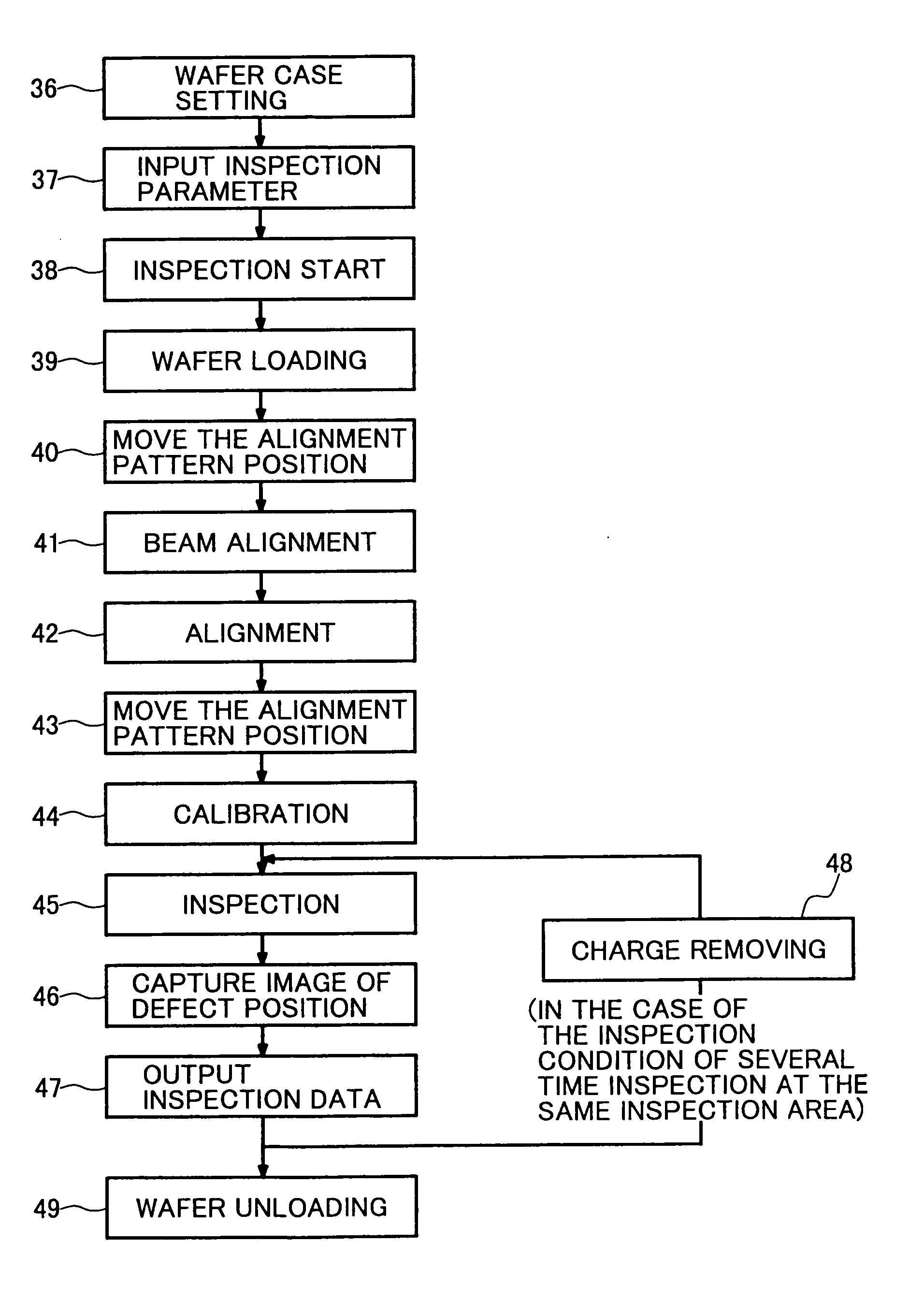
[0048] According to the embodiment, a description will be given of an inspection method and an inspection system for inspecting presence or absence of leakage failure with regard to a semiconductor wafer in the midst of steps of fabricating thereof.

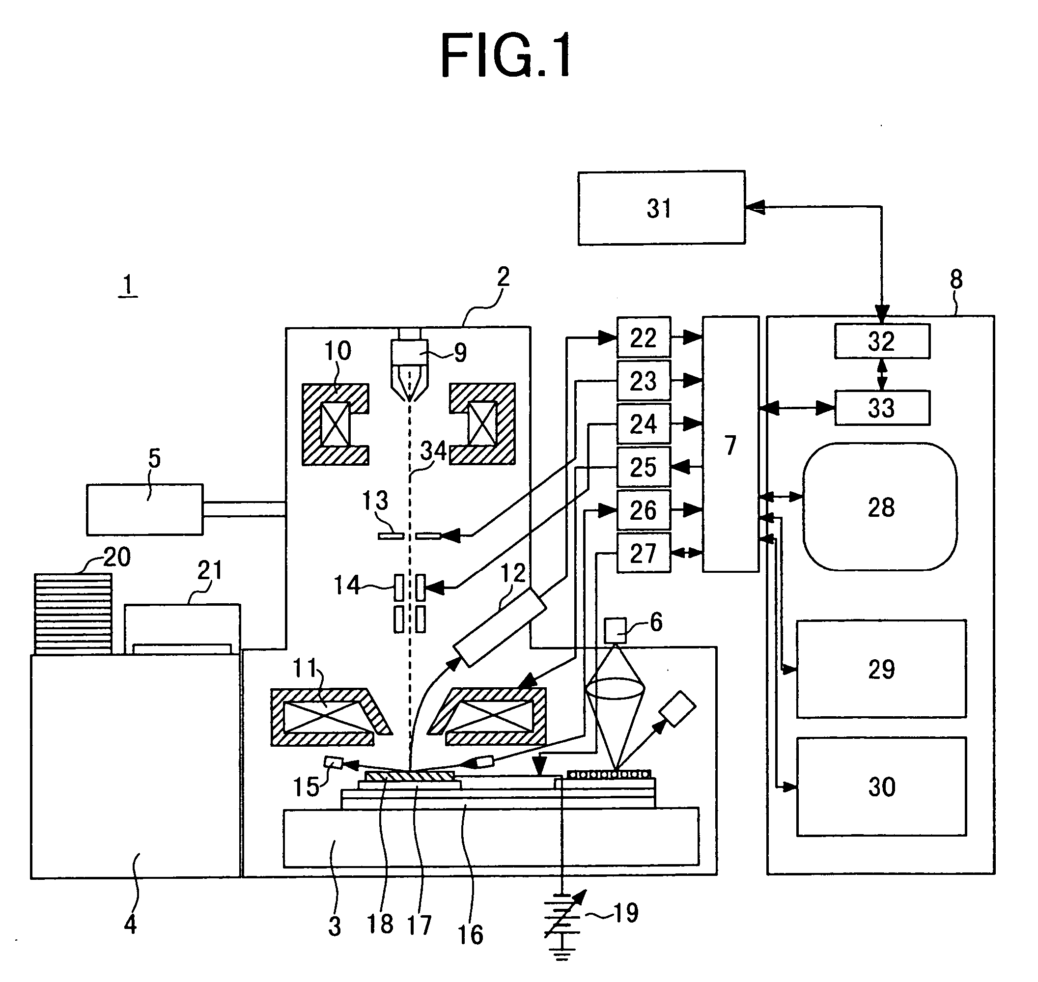
[0049] First, FIG. 1 shows a constitution of an inspection system of a semiconductor device according to the embodiment. An inspection system 1 of a semiconductor device is constituted by an electron beam optics unit 2, a stage mechanism unit 3, a wafer handling unit 4, a vacuum unit 5, an optical microscope unit 6, a control unit 7 and a control unit 8.

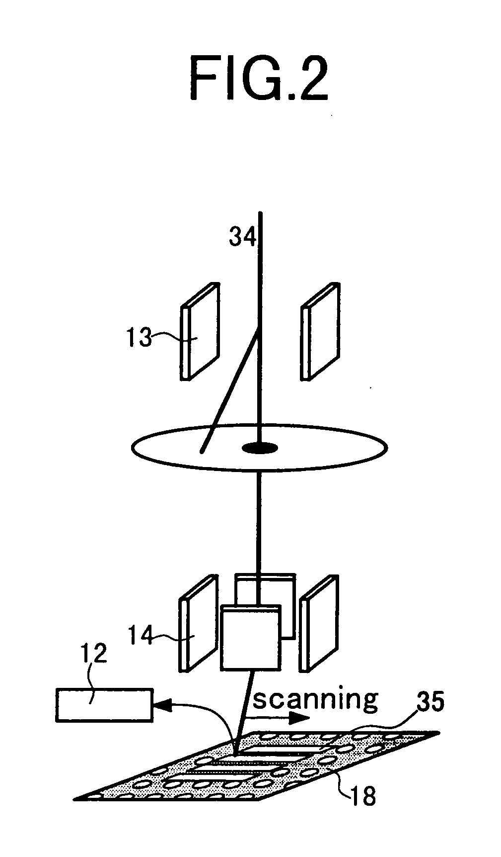
[0050] The electron beam optics unit 2 is constituted by an electron gun 9, a condenser lens 10, an objective lens 11, a detector 12, a blanking deflector 13, a deflector 14 and a wafer height measure sensor 15.

[0051] The stage mechanism unit 3 is constituted by an XY stage 16 and a holder 17 for mounting a wafer, and a retarding power supply 19 for applying negative voltage on the hold...

embodiment 2

[0075] According to a second embodiment, the result of inspection in the first embodiment is displayed by a probability. FIG. 11 shows an example of display of the probability. Although the probability can be calculated by bit numbers at respective retention time period, in an actual inspection, it is substantially impossible to execute an inspection in correspondence with all of the retention time periods. Hence, according to the embodiment, by combining various inspection parameters explained in the first embodiment, there are set inspection conditions in correspondence with three kinds of retention time periods and the inspection is executed. As a result of inspection by a first inspection condition, there are detected bits of a retention time period in correspondence with numeral 65 of FIG. 11, the result is inputted to the probability and by a similar method, there are calculated bit numbers of retention time periods in correspondence with numeral 66 of FIG. 11 and numeral 67 o...

embodiment 3

[0077] According to a third embodiment, there is shown an example in which the invention is applied to a leakage failure inspection of a flash memory product. According to a flash memory, accumulation and erasure of charge is executed via a floating gate. Therefore, when there is present a defect at an oxide film between the gate and a substrate and leakage is caused, a failure is constituted. By applying the inspection method, leakage failure between the gate and the substrate can be detected. Further, in the case of causing leakage between the source and the drain, when the cause is derived from crystal failure, by inspecting a plug pattern on the substrate, portions of causing the leakage failure can be specified.


PUM


Abstract

Electron beam is irradiated to a wafer in the midst of steps at predetermined intervals by a plurality of times under a condition in which a junction becomes rearward bias and a difference in characteristic of a time period of alleviating charge in the rearward bias is monitored. As a result, charge is alleviated at a location where junction leakage is caused in a time period shorter than that of a normal portion and therefore, a potential difference is produced between the normal portion and a failed portion and is observed in a potential contrast image as a difference in brightness. By consecutively repeating operation of acquiring the image, executing an image processing in real time and storing a position and brightness of the failed portion, the automatic inspection of a designated region can be executed. Information of image, brightness and distribution of the failed portion is preserved and outputted automatically after inspection.

Description

BACKGROUND OF THE INVENTION [0001] The present invention relates to a method and an apparatus of fabricating a substrate having a fine circuit pattern such as semiconductor device or liquid crystal, particularly to a technology of inspecting a semiconductor device and relates to a technology of evaluating electric properties by a wafer in the midst of a procedure of fabricating a semiconductor device and an inspection technology for carrying out defect analysis on electric properties of a wafer finished with fabricating steps. [0002] An explanation will be given of inspection of a semiconductor wafer as an example. [0003] It is necessary that a semiconductor device stores data written to a transistor for a predetermined period of time. For such purpose, there is formed a junction on a surface of a substrate and electric charge stored in the transistor is prevented from being leaked under a condition other than predetermined potential. When leakage failure (retention failure) occurs,...

Claims


Application Information

Patent Timeline
Patent Type & Authority Applications(United States)
IPC IPC(8): G01Q10/00G01R31/28G01Q30/04G01R31/307H01L21/00H01L21/66
CPCG01R31/307H01J37/222H01J37/256H01J37/263H01J37/265H01J2237/304H01J2237/043H01J2237/24564H01J2237/2594H01J2237/2813H01J2237/2817H01J37/266
Inventor NOZOE, MARI
Owner HITACHI LTD
Why Eureka
Try Eureka