Method of etching a porous dielectric material

a dielectric material and porous technology, applied in the field of porous dielectric materials, can solve the problems of material deformation, failure of devices produced, modification of porous and hybrid dielectric materials during production, etc., and achieve the effects of reducing or even eliminating damage and/or formation, low permittivity, and promoting the conduction of filling materials

Active Publication Date: 2015-09-24
COMMISSARIAT A LENERGIE ATOMIQUE ET AUX ENERGIES ALTERNATIVES
View PDF17 Cites 3 Cited by
  • Summary
  • Abstract
  • Description
  • Claims
  • Application Information

AI Technical Summary

Benefits of technology

[0013]Particularly advantageously, the etching step of the method according to the invention makes it possible to form a trench, the flanks and bottom of which are devoid of residues. Thus, during the step of filling the trenches, limiting residual deposits on the flanks improves the conduction quality of the filling material and thereby promotes the reliability of the interconnection lines.
[0015]Particularly advantageously, the protective layer based on hydrocarbon that develops during etching protects the porous dielectric material from any contamination or modification.
[0016]Preferably, the mixture of gas forming the plasma also comprises nitrogen (N2) or oxygen (O2). In addition, the nitrogen makes it possible to etch the porous dielectric material and to control the quantity of carbon deposited on the flanks.
[0019]Thus, according to a non-limitative embodiment, the pattern forms a trench. According to another non-limitative embodiment, the pattern can serve to remove the layer of porous dielectric material outside the flanks of the gate in order to leave spacers in place.
[0022]The aim of the invention is to develop a method for producing interconnection lines also comprising a step of chemical etching of a layer of porous dielectric material forming a trench. Advantageously, this etching step reduces or even eliminates damage and / or the formation of residues on the front of the layer of porous dielectric material.
[0023]Advantageously, the formation of a protective layer on the flanks of the layer of porous dielectric material enables the porous dielectric material to keep its electrical properties and in particular low permittivity. Particularly advantageously, limiting residual deposits and forming a protective layer on the flanks of the layer of porous dielectric material make it possible to promote the conduction of the filling material and thus improve the reliability of the interconnection lines.

Problems solved by technology

Furthermore, producing narrow trenches in the porous dielectric material, SiOCH for example, requires reviewing the various plasma methods (etching, post-etching treatments) and integration schemes, since this material is known to be easily degraded when it is exposed to a plasma based on fluorine in particular.
One major problem is the modification of porous and hybrid dielectric materials during “post-etching” plasma.
The main drawback of a plasma etching based on fluorine in a device comprising a metal hard mask and a layer of porous dielectric material is the generation of residues resulting from the interaction between the chemical species present in the plasma and on the metal mask; said residues are deposited on the layers and consequently cause failures of the devices produced.
Moreover, problems of absorption of moisture are also encountered, which could give rise to an increase in the dielectric constant of the low-permittivity dielectric material; which runs counter to the aim sought and also affects the reliability of the device produced.
These residues 170 may produce unwanted vias between lines (for example short-circuits) and line ruptures (for example open circuits) that very significantly affect the manufacturing yield of the devices produced.
FIG. 1c illustrates yet another problem that is related to wet cleaning based on the use of hydrofluoric acid (HF) and which proves not to be sufficiently effective to eliminate all the fluorocarbon layer formed during etching.
The fluorine has a tendency to diffuse and may lead to a degradation in reliability of the porous dielectric material 140, for example a p-SiOCH.
An aggressive wet cleaning, which would remove all of the fluorine layer, would have the drawback of leading to a loss of definition of the critical dimensions of the devices produced.
Consequently, introducing low-permittivity porous dielectric materials necessary for reducing the time constant of the interconnections between active components of an integrated circuit, and in particular etching these porous dielectric materials in a fluorocarbon plasma, pose numerous problems.

Method used


Image

  • Method of etching a porous dielectric material
  • Method of etching a porous dielectric material
  • Method of etching a porous dielectric material

Examples


Embodiment Construction

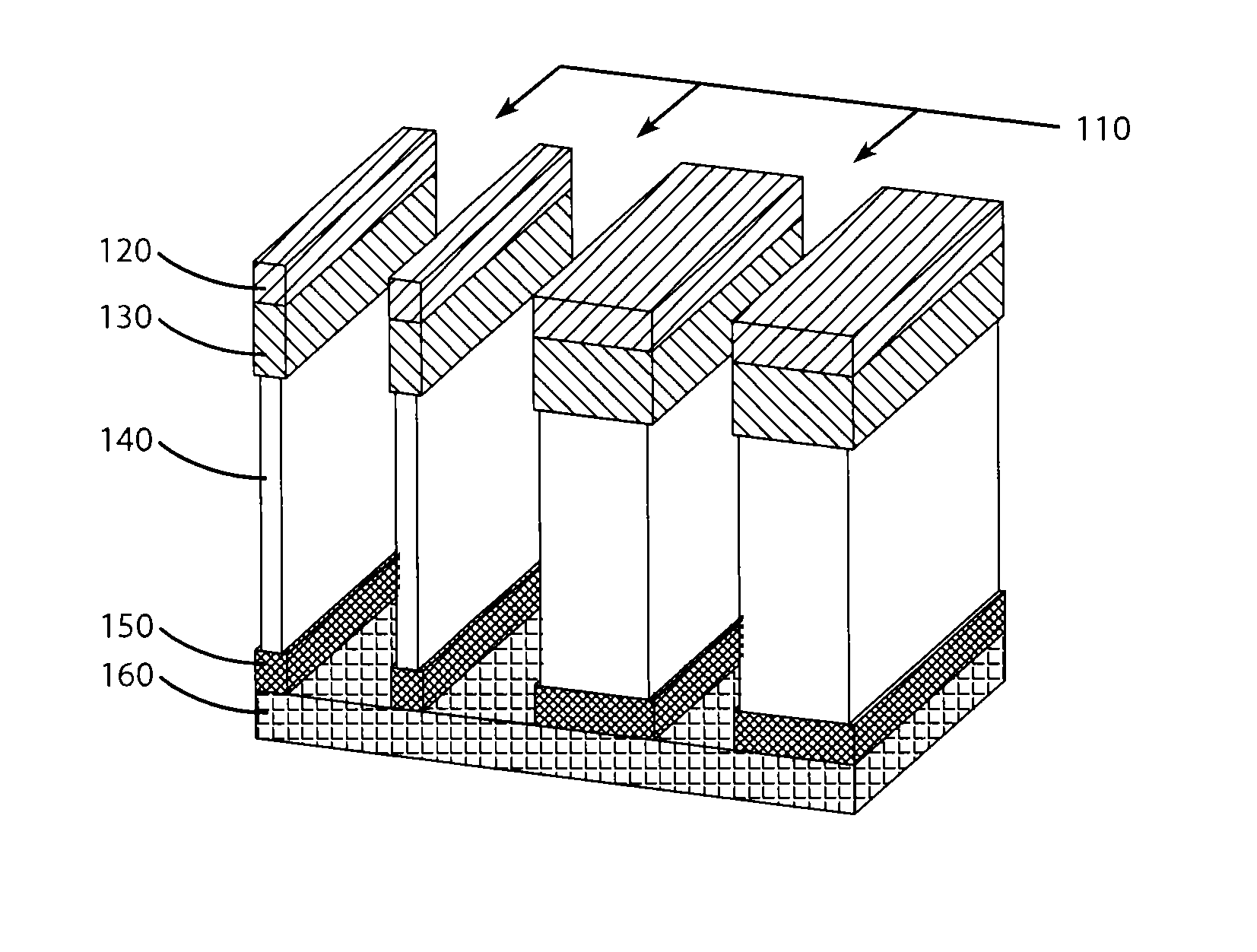
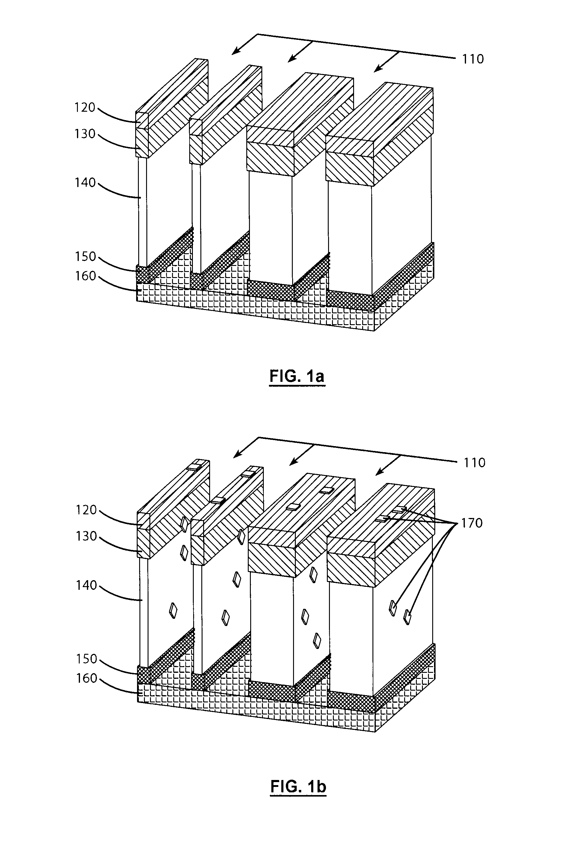
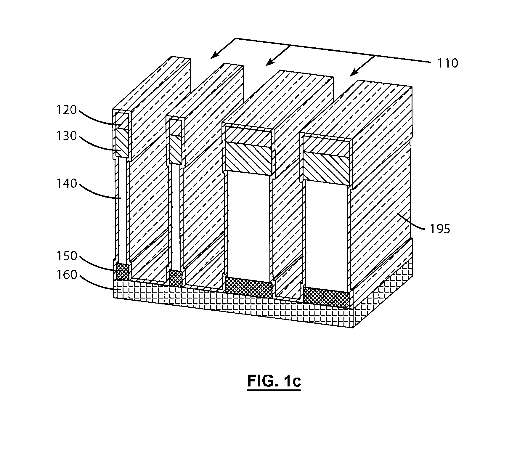
[0030]In the context of the present invention, the term “on” or “underlying” does not necessarily mean “in contact with”. Thus, for example, depositing a first layer on a second layer does not necessarily mean that the two layers are directly in contact with each other but means that the first layer at least partially covers the second layer while being either directly in contact therewith or being separated therefrom by another layer or another element.

[0031]In the following description, the thicknesses are generally measured in directions perpendicular to the plane of the bottom face of the layer to be etched or of a substrate on which the bottom layer is disposed. Thus the thicknesses are generally taken in a vertical direction on the figures depicted. On the other hand, the thickness of a layer covering a flank of a pattern is taken in a direction perpendicular to this flank.

[0032]Before beginning a detailed review of embodiments of the invention, optional features, which may op...


PUM

PropertyMeasurementUnit
thicknessesaaaaaaaaaa

Abstract

A method for producing interconnection lines including etching a layer of porous dielectric material forming a trench and filling the trench is provided. The etching is carried out in a plasma so as to grow, all along the etching, a protective layer on flanks of the layer of porous dielectric material. The plasma is formed from a gas formed from a first component and a second component, or a gas formed from a first component, a second component and a third component. The first component is a hydrocarbon of the CXHY type, where X is the proportion of carbon in the gas and Y the proportion of hydrogen in the gas; the second component is taken from nitrogen or dioxygen or a mixture of nitrogen and dioxygen; the third component is taken from argon or helium; and the protective layer is based on hydrocarbon.

Description

FIELD OF THE INVENTION[0001]The present invention relates to the use of porous dielectric materials with low permittivity for producing electrical interconnection lines for microelectronic devices and in particular in integrated circuits. It relates more particularly to an improved method for etching such materials.TECHNOLOGICAL BACKGROUND[0002]In order to reap the requirements for size of the devices and switching times in microelectronics, the method for producing interconnection lines, said lines requiring insulation by a porous dielectric material, has had to be adapted. Furthermore, producing narrow trenches in the porous dielectric material, SiOCH for example, requires reviewing the various plasma methods (etching, post-etching treatments) and integration schemes, since this material is known to be easily degraded when it is exposed to a plasma based on fluorine in particular. The studies carried out to evaluate the efficacy of various plasmas according to the materials expose...

Claims


Application Information

Patent Timeline
Patent Type & Authority Applications(United States)
IPC IPC(8): H01L21/768H01L21/033
CPCH01L21/76802H01L21/0332H01L21/76829H01L21/0337H01L21/0335H01L21/31116H01L21/31144H01L21/76811H01L21/76831H01L21/02126H01L21/76826
Inventor POSSEME, NICOLAS
Owner COMMISSARIAT A LENERGIE ATOMIQUE ET AUX ENERGIES ALTERNATIVES
Why Eureka
Try Eureka