Probe cleaning sheet and cleaning method

a technology of cleaning sheet and probe, which is applied in the direction of instruments, semiconductor/solid-state device testing/measurement, manufacturing tools, etc., can solve the problems of affecting the cleaning effect of the probe tip end, and affecting the cleaning effect of the probe. , to achieve the effect of soft and efficient cleaning and sufficient cushioning property

Inactive Publication Date: 2005-11-17
SUMITOMO ELECTRIC IND LTD
View PDF0 Cites 57 Cited by
  • Summary
  • Abstract
  • Description
  • Claims
  • Application Information

AI Technical Summary

Benefits of technology

[0021] An object of the present invention is to provide a probe cleaning sheet having a layered structure including a polishing layer and an elastic layer arranged therebelow, for removing, by a contact with the polishing layer, foreign matter adhered to a tip end of a probe for semiconductor inspection exhibiting sufficient cushioning property for use not only in room and high temperature environments but also in low temperature environment, and capable of softly and efficiently cleaning the tip end of the probe. Another object is to provide a method of cleaning for removing foreign matter adhered to a tip end of a probe for semiconductor inspection in such a low temperature environment.

Problems solved by technology

Adhesion of foreign matter such as aluminum powder to the tip end of the probe causes conduction failure between the probe and the pad, or degrades electrical contact, hindering accurate measurement of electrical characteristics of the semiconductor chip.
Further, adhesion of foreign matter to the tip end of the probe results in fluctuation of contact resistance of the probe.
In the method using a ceramic plate, however, the tip end of the probe tends to be scraped away, so that life of the probe card, which is expensive, becomes shorter.
When the tip end of the probe is scraped away through repetitive cleaning and the tip end that has been spherical come to have a flat shape, it becomes difficult to realize smooth contact between the probe and the pad.
This method, however, has a disadvantage that fragments of the cleaning member as new foreign matter adhere to the tip end of the probe, or the tip end of the probe is damaged at the time of piercing.
Further, foreign matter such as aluminum powder accumulates in the cleaning member, and therefore, cleaning performance degrades quickly.
Further, even when the prove tip end is brought into press-contact with the polishing layer, the polishing layer is not readily be torn.
The known cleaning sheet, however, employs silicone rubber or urethane rubber (polyurethane) as the elastic layer, and therefore, elasticity (cushioning property) of the elastic layer significantly degrades in a low temperature environment.
As a result, amount of wear of the probe tip end increases when cleaned in the low temperature environment, and the life of probe card becomes shorter.

Method used


Image

  • Probe cleaning sheet and cleaning method
  • Probe cleaning sheet and cleaning method

Examples


example 1

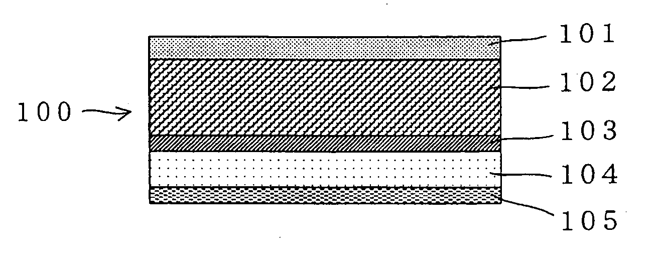
[0069] A coating liquid (solid content concentration: 50 mass %) was prepared by dispersing 40 mass % of silicon carbide (#4000: grain size 3 μm) in aqueous suspension (PFA concentration: 10 mass %) of tetrafluoro-ethylene-perfluoroalkyl vinyl ether copolymer (PFA). On one surface of a drawn PTFE porous body film having porosity of 70%, average pore diameter of 0.3 μm and thickness of 800 μm, a PET film (thickness: 10 μm) was provided by thermal fusion, to form a laminated body. On the surface of drawn PTFE porous film opposite to the PET film, the coating liquid was applied and dried, to form a polishing layer having the thickness of 50 μm. On a surface of the PET film, an epoxy-based adhesive was applied and dried, to form an adhesive layer (thickness: 90 μm). The adhesive layer was semi-cured by heating at 80° C. for 5 minutes. On the adhesive layer, releasing paper (polyethylene-coated quality paper) was placed, and the resulting body was cut to a cleaning sheet A (thickness of ...


PUM

PropertyMeasurementUnit
pore diameteraaaaaaaaaa
porosityaaaaaaaaaa
grain diameteraaaaaaaaaa

Abstract

A probe cleaning sheet is provided, which can be used not only at a room temperature and high temperature but also in a low temperature environment with sufficient cushioning property and which can softly and efficiently clean a probe tip end. Specifically, the cleaning sheet has a layered structure including an elastic layer below a polishing layer, for removing, by contact with the polishing layer, foreign matter adhered on a tip end of a probe for semiconductor inspection, and the elastic layer is a polytetrafluoro-ethylene porous body layer.

Description

BACKGROUND OF THE INVENTION [0001] 1. Field of the Invention [0002] The present invention relates to a probe cleaning sheet for removing foreign matter adhered to a tip end of a probe for inspecting a semiconductor used for testing (inspecting) electrical characteristics of a semiconductor chip. The present invention further relates to a method of cleaning the probe for inspecting a semiconductor using the cleaning sheet in a low temperature environment. [0003] 2. Description of the Background Art [0004] In the process of manufacturing semiconductors, defective and non-defective semiconductor chips on which circuit patterns have been formed are sorted using a wafer prober that physically and electrically connects a pad (electrode portion) of a semiconductor chip to a tester. A wafer prober adopting a probe is commonly used. Specifically, as a wafer prober, an apparatus is known in which a probe is brought into contact with a pad of a semiconductor chip (electronic circuit die) such ...

Claims


Application Information

Patent Timeline
Patent Type & Authority Applications(United States)
IPC IPC(8): G01R31/26B08B1/00B24B1/00B24D15/02B32B27/08G01R1/06G01R3/00G01R31/28H01L21/66
CPCB08B1/00G01R3/00B32B27/08B24D15/023H01L21/304B32B5/16B32B7/06B32B27/14B32B27/322B32B2255/04B32B2260/025B32B2305/02B32B2457/00
Inventor HAGA, TSUYOSHI
Owner SUMITOMO ELECTRIC IND LTD
Why Eureka
Try Eureka