Semiconductor device, method for mounting the same, and method for repairing the same

a semiconductor and device technology, applied in the field of semiconductor devices, can solve problems such as failures of semiconductor devices, cracks or chips in sealant, and failures of mounting devices, and achieve the effect of reducing the occurrence rate of semiconductor device failures

Inactive Publication Date: 2005-11-24
LAPIS SEMICON CO LTD
View PDF0 Cites 35 Cited by
  • Summary
  • Abstract
  • Description
  • Claims
  • Application Information

AI Technical Summary

Benefits of technology

[0011] The present invention has been made to solve the above-mentioned problem of the prior art and has as its object to provide a method for mounting a semiconductor device, which can reduce the occurrence rate of semiconductor device failures, such as the popcorn phenomenon mentioned above, and provide a semiconductor device that makes this mounting method viable.
[0012] Another object of the present invention is to provide a semiconductor device repair method for easily repairing a failure of the solder joint in a semiconductor device without changing the semiconductor device, and also provide a semiconductor device that makes this repair method feasible.

Problems solved by technology

Incidentally, in the mounting process of a semiconductor of BGA structure, mounting-induced faults sometimes occur.
If this phenomenon occurs, there is a possibility that the sealant cracks or the chip separates from the sealant.
A problem here is that the detached semiconductor device is not reutilized and goes down the drain.

Method used


Image

  • Semiconductor device, method for mounting the same, and method for repairing the same
  • Semiconductor device, method for mounting the same, and method for repairing the same
  • Semiconductor device, method for mounting the same, and method for repairing the same

Examples


first embodiment

Modification of First Embodiment

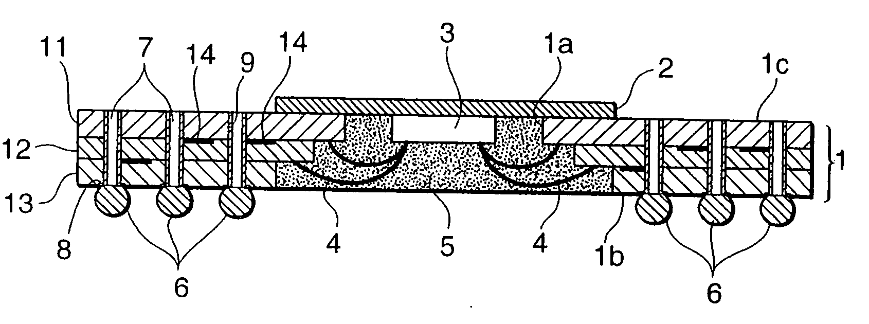
[0089]FIG. 14 is a sectional view showing a modification of the first embodiment. In this semiconductor device, each through-hole 7 is filled with a filling material 15. For the filling material 15, it is possible to use materials which have elasticity and non-heat-conductivity, like gel resins which do not exhibit fluidity after the through-hole 7 is filled, such as a silicon-based resin “JCR6110” by Toray Industries, Inc. or a polyimide-based resin “PIX8200” by Hitachi Chemical Co., Ltd. The filled portion 15 is formed by injecting a gel resin from the upper side of the openings of the through-holes 7. As shown in FIG. 14, by the provision of the filled portion 15 in the through-hole 7, it is possible to prevent failures ascribable to corrosion, for example, of the joint between the terminal 8 and the solder ball 6, and also preclude the occurrence of failures resulting from the infiltration of foreign matter into the through-holes 7 from outside.

[...

second embodiment

[0091]FIG. 15(a) is a sectional view schematically showing the through-hole and its vicinity of the semiconductor device according to a second embodiment of the present invention. FIG. 15(b) is a plan view showing the through-hole and the vicinity on an enlarged scale.

[0092] The difference from the semiconductor device according to the first embodiment is that an electrode 16 as an electrical conductor is formed in the shape of a semi-circular column within the through-hole 7 in the semiconductor device of the second embodiment. For forming the conductor made by an electrode material 16, it is possible to adopt a method of manufacturing a semicircular column part, setting this column part in each through-hole of the substrate 1, and forming an electrode 16 that fills up the clearance between the column part and the through-hole 7, and then extracting the semi-circular electrode 16. According to the semiconductor device of the second embodiment, the electrode 16 is additionally conn...

third embodiment

[0096]FIG. 17(a) is a sectional view schematically showing a through-hole and its vicinity of a semiconductor device according to a third embodiment of the present invention, and FIG. 17(b) is a plan view showing the terminal 31 of the substrate 1.

[0097] The only difference from the semiconductor device of the first embodiment is that a semi-cylindrical opening 31a is provided in the terminal 31 as shown in FIG. 17(b) in the semiconductor device in the third embodiment. According to the semiconductor device of the third embodiment, the bond area between the solder ball 6 and the terminal 31 is increased and the bond strength of the solder ball is increased.

[0098] The repair method and the mounting method of the semiconductor device according to the third embodiment are the same as those in the first embodiment.

[0099] A filler of gel resin may be provided that fills up the through-hole of the semiconductor device according to the third embodiment.

[0100]FIG. 18(a) is a sectional v...


PUM


Abstract

A method for mounting a semiconductor device, which can decrease the occurrence rate of failures, a method for repairing a semiconductor device, which can easily repair defective solder joints, and a semiconductor device which makes those methods feasible. A substrate 1 has formed therein through-holes 7 lined on the internal walls with a wiring layer 9, and solder balls 6 are fusion-bonded to the substrate 1 in such a manner as to cover the through-holes 7. In the mounting process or in the repair process, heating probes 41 are passed through the through-holes 7 and thrust into the solder balls 6 to thereby melt the solder balls, and the heating probes are pulled out of the solder balls to let the solder balls cool down. In those processes, only the solder balls 6 can be heated, thereby averting adverse effects on the IC chip 3. In the repair process, the solder balls 6 can be restored to an initial condition free of intermetallic compounds.

Description

FIELD OF THE INVENTION [0001] The present invention relates to a semiconductor device of ball grid array package (BGA) structure, a method for mounting the semiconductor device, and a method for repairing the semiconductor device. PRIOR ART [0002]FIG. 26 is a sectional view schematically showing a conventional semiconductor device of BGA structure of a cavity down type. [0003] As shown in FIG. 26, the conventional semiconductor device comprises a substrate 101 having an electric wiring circuit formed therein, and a heat slug 102 formed by a copper sheet or the like glued by an adhesive to a periphery of a center opening 101 of the substrate 101. The conventional semiconductor 20 device comprises an IC chip glued by an adhesive to the heat slug, a metal thin line 104 electrically connecting the IC chip 103 and wiring on the substrate 101, a sealant 105, such as an epoxy resin, for sealing the IC chip 103 and the metal thin line 104, and solder balls 106 as external terminals arrayed ...

Claims


Application Information

Patent Timeline
Patent Type & Authority Applications(United States)
IPC IPC(8): H01L23/12H01L21/60H01L23/498H01L23/58H05K3/22H05K3/34H05K3/42
CPCH01L22/32H01L2924/3651H01L23/49805H01L23/49816H01L23/49827H01L2224/48091H01L2224/49109H01L2924/01078H01L2924/01079H01L2924/15311H01L2924/1532H05K3/225H05K3/3436H05K3/429H05K2201/0394H05K2201/0959H05K2201/0969H05K2201/09736H05K2201/10666H05K2203/0195H01L23/498H01L24/49H01L2924/01327H01L24/48H01L2924/00014H01L2224/05599H01L2224/45099H01L2224/85399H01L2924/181Y02P70/50H01L2224/45015H01L2924/207H01L2924/00012
Inventor NOGUCHI, TAKASHI
Owner LAPIS SEMICON CO LTD
Why Eureka
Try Eureka