Switching power source device

a power source and switching technology, applied in the direction of electric variable regulation, process and machine control, instruments, etc., can solve the problems of reducing the conversion efficiency of the light load period, reducing and reducing the oscillation frequency of the drive signal. , the effect of improving the conversion efficiency of the switching power sour

Inactive Publication Date: 2005-11-24
SANKEN ELECTRIC CO LTD
View PDF5 Cites 63 Cited by
  • Summary
  • Abstract
  • Description
  • Claims
  • Application Information

AI Technical Summary

Benefits of technology

[0007] The switching power source according to the present invention comprises a DC power source (1); a primary winding (2a) of a transformer (2) and a switching element (3) connected in series to the DC power source (1); a current detector (9) for acquiring electric current (ID) flowing through the primary winding (2a) of the transformer (2) or the switching element (3); a rectifying smoother (6) connected to a secondary winding (2b) of the transformer (2) for generating DC output voltage (VOUT); and a control circuit (8) for supplying the switching element (3) with drive signals (VG) to turn the switching element (3) on and off so as to keep the DC output voltage (VOUT) on a substantially constant level. The control circuit (8) comprises a current comparator (27) for comparing a voltage level of signals acquired by the current detector (9) with a reference voltage level (VDT) to produce detection signals (VCP) of first or second level (L or H); an edge detector (28a) for sensing an edge of drive signal (VG) supplied to a control terminal of the switching element (3) during the period of transition from turning on to off of the switching element (3); and a decision means (28b) for receiving a current detection signal (VCP) from the current comparator (27) to produce an output signal (VLD) when the edge detector (28a) catches an edge of drive signal (VG); wherein the decision means (28b) produces the different output signals (VLD) of respectively first and second voltage levels (L and H) under the light load condition and non-light load condition heavier than light load. Accordingly, the decision means (28b) can correctly appreciate the load condition based on output signals of the current detector (9) at the transitional time of turning the switching element (3) from on to off, without any error in the decision resulted from capacitative short-circuit current such as surge current which may occur at the time of turning on of the switching element (3) so that the load condition on the secondary side of the transformer (2) can precisely and certainly be detected on the primary side of the transformer (2). Also, the decision on the load condition is hardly susceptive to influences of foreign noise such as inductive noise.
[0008] In a first embodiment of the present invention, the control circuit (8) is provided with an oscillation controller (22) which reduces the oscillation frequency of drive signals (VG) when the decision means (28b) produces the output signal (VLD) of the first voltage level (L), and adversely, increases the oscillation frequency of drive signals (VG) when the decision means (28b) produces the output signal (VLD) of the second voltage level (H). Under the light load condition, a small amount of electric current (ID) flows through the primary winding (2a) of the transformer (2) or switching element (3) so that the decision means (28b) generates the output signal (VLD) of the first voltage level (L) which reduces the oscillation frequency of drive signals (VG) applied to the control terminal of the switching element (3) from the oscillation controller (22) to lower the switching number of the switching element (3). This allows decrease in switching loss during the light load period and also enhancement in conversion efficiency of the switching power source in a wider load fluctuation range.
[0011] A fourth embodiment of the present invention comprises a plurality of current comparators (27, 62), a plurality of edge detectors (28a) and a plurality of decision means (28b, 63) wherein the current comparators (27, 62) compare a detection signal (VOCP) by current detector (9) with levels of different reference voltages (VDT1, VDT2) to reduce oscillation frequency of drive signals (VG) to different frequencies by output signals (VLD1, VLD2) of the first level of the voltage output from the decision means (28b, 63). Under the light load condition, oscillation frequency of drive signals (VG) applied to the control terminal of the switching element (3) can be lowered to different frequencies in response to the load condition to accomplish fine control of the oscillation frequency and improve conversion efficiency of the switching power source.
[0012] In a fifth embodiment of the present invention, the control circuit (8) comprises an intermittent oscillation controller (71) for suspending the on-off operation of the switching element (3) for a given period of time sufficiently longer than an oscillation cycle of the drive signals (VG) when the decision means (28b) produces the output signal (VLD) of the first voltage level (L). Under the light load condition wherein smaller electric current (ID) flows through the primary winding (2a) of the transformer (2) or switching element (3), the output signal (VLD) of the decision means (28b) is on the first voltage level (L) to cease the on-off operation of the switching element (3) by the intermittent oscillation controller (71) for a certain period of time (tB) perfectly longer than the oscillation cycle of the drive signals (VG), extremely reducing the switching number of the switching element (3). This allows steep reduction in the switching loss under the light load mode and attains enhancement in conversion efficiency of the switching power source in a wider load fluctuation range.

Problems solved by technology

A known switching power source of self-induced flyback type such as RCC (ringing choke converter) is defective in that it increases on-off switching frequency of a switching element when an electric load becomes light because the on-period of the switching element becomes shorter with the shorter period of producing flyback voltage on a secondary winding of a transformer.
Thus, with the lighter load, the number of times the switching element is turned on and off is increased, resulting in augmentation of switching loss and reduction of conversion efficiency during the light load period.
However, as electric loss other than switching loss is decreased during the light load period, switching loss occupies a major proportion, reducing the conversion efficiency.
This switching power source is advantageous because it reduces switching loss in the stand-by mode or during the light load period, thereby resulting in improved conversion efficiency, however disadvantageous because it requires increased number of required components that causes rise in cost of manufacture.
Also, it is actually impossible to apply the switching power source to AC adaptors for small electronic devices such as mobile phones or personal handy phone systems or portable personal computers because the power source involves a large-scale addresser such as a microcomputer.
However, in any event, these arrangements have a drawback of increase in number of required components for assembly.
This technique, however, unfavorably may cause capacitative short-circuit over-current to flow through the switching element at the moment of turning it on as shown in FIG. 27 due to a parasitic capacitance formed by an inherent structure in the switching element; a snubber circuit (such as a capacitor) connected between two electrodes of the switching element for reduction of noise or another snubber circuit connected between windings of transformer to reduce noise and protect the switching element.
The capacitative short-circuit over-current disturbs the accurate detection of secondary load condition because the over-current cannot be determined only by the secondary load condition, and moreover, a peak value of the over-current may be elevated over a peak value of a secondary load current during the light load period.
Accordingly, such a prior art switching power source makes it very difficult to exactly detect the secondary load condition on the primary side with minimum number of required components in order to select an optimal oscillation operation based on the detection result on the primary side and thereby improve the conversion efficiency of the power source.

Method used


Image

  • Switching power source device
  • Switching power source device
  • Switching power source device

Examples


Embodiment Construction

[0042] Embodiments of the switching power source according to the present invention will be described hereinafter in connection with FIGS. 1 to 25 of the drawings.

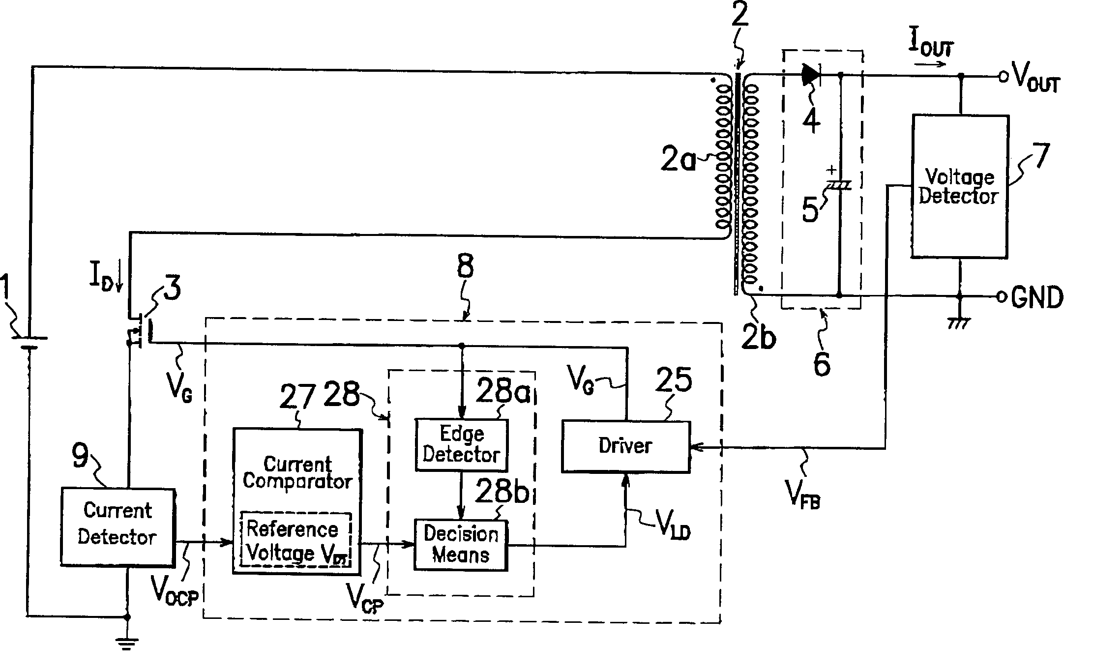
[0043]FIG. 1 is a block circuit diagram indicating a basic concept of a switching power source according to each embodiment of the present invention. The switching power source shown in FIG. 1 comprises a DC power source 1; a primary winding 2a of a transformer 2 and a switching element or MOS-FET (Field Effect Transistor of MOS type) 3 connected in series to DC power source 1; a rectifying smoother 6 which comprises a rectifying diode 4 connected to a secondary winding 2b of transformer 2 and a smoothing capacitor 5 to generate DC output voltage VOUT; a voltage detector (output voltage detecting circuit) 7 for sensing DC output voltage VOUT; a control circuit 8 which comprise a driver 25 for receiving detection signals VFB from voltage detector 7 and supplying MOS-FET 3 with drive signals VG to turn MOS-FET 3 on and off ...


PUM


Abstract

A switching power source comprises a current comparator 27 for comparing a voltage level of signals acquired by a current detector 9 with a reference voltage level VDT to produce detection signals VCP of first or second level L or H; an edge detector 28a for sensing an edge of drive singal VG supplied to a gate terminal of MOS-FET 3 during the period of transition from turning on to off of MOS-FET 3; and a decision means 28b for receiving a current detection signal VCP from current comparator 27 to produce an output signal VLD when edge detector 28a catches an edge of drive signal VG; wherein decision means 28b produces different output signals VLD of respectively first and second voltage levels L and H under the light and heavy load conditions to precisely and certainly detect on the primary side of transformer 2 the load condition on the secondary side of transformer 2 for improvement in conversion efficiency.

Description

TECHNICAL FIELD [0001] This invention relates to a switching power source, in particular, of the type wherein a primary side of a transformer can serve to accurately and reliably detect an electrical load condition on a secondary side to improve the conversion efficiency. BACKGROUND OF THE INVENTION [0002] A known switching power source of self-induced flyback type such as RCC (ringing choke converter) is defective in that it increases on-off switching frequency of a switching element when an electric load becomes light because the on-period of the switching element becomes shorter with the shorter period of producing flyback voltage on a secondary winding of a transformer. A typical on-off switching frequency or oscillation frequency of switching element generally ranges from 30 to 70 kHz under the maximum load and from 200 to 400 kHz under the minimum load. Thus, with the lighter load, the number of times the switching element is turned on and off is increased, resulting in augmen...

Claims


Application Information

Patent Timeline
Patent Type & Authority Applications(United States)
IPC IPC(8): H02M3/335
CPCH02M2001/0025H02M3/33523H02M1/0025H02M3/28
Inventor KOIKE, KENGO
Owner SANKEN ELECTRIC CO LTD
Why Eureka
Try Eureka