SOI circuit having reduced crosstalk interference and a method for forming the same

a technology of crosstalk interference and silicon on the insulator, which is applied in the direction of basic electric elements, electrical equipment, semiconductor devices, etc., can solve the problems of difficult integration of components performing different functions on the same chip, weak performance of a chip or a unit comprising different components, and high interference, so as to reduce interference, reduce interference, and high performance

Inactive Publication Date: 2005-11-24
PIZZARULLI ANDREA
View PDF14 Cites 7 Cited by
  • Summary
  • Abstract
  • Description
  • Claims
  • Application Information

AI Technical Summary

Benefits of technology

[0011] In general, the present invention is directed to a method allowing the formation of isolated portions on a substrate so as to reduce the crosstalk interference between those portions of a circuit which are formed on these isolated portions of the substrate. In more detail, the present invention is directed to a method of disposing portions of a circuit on a substrate, wherein said method allows to reduce the crosstalk interference between the circuit portions and to a circuit on a substrate exhibiting very low crosstalk interference.
[0012] The present invention is based on the following consideration. Very high performances (in terms of reduced crosstalk interference) may be obtained also in the case of circuits fabricated on a thick silicon layer according to standard bulk CMOS and / or BiCMOS technologies. Accordingly, for all those applications for which standard CMOS and / or BiCMOS fabricating technologies may be preferred to the usual SOI technology (offering very high performances in terms of high speed and / or reduced 
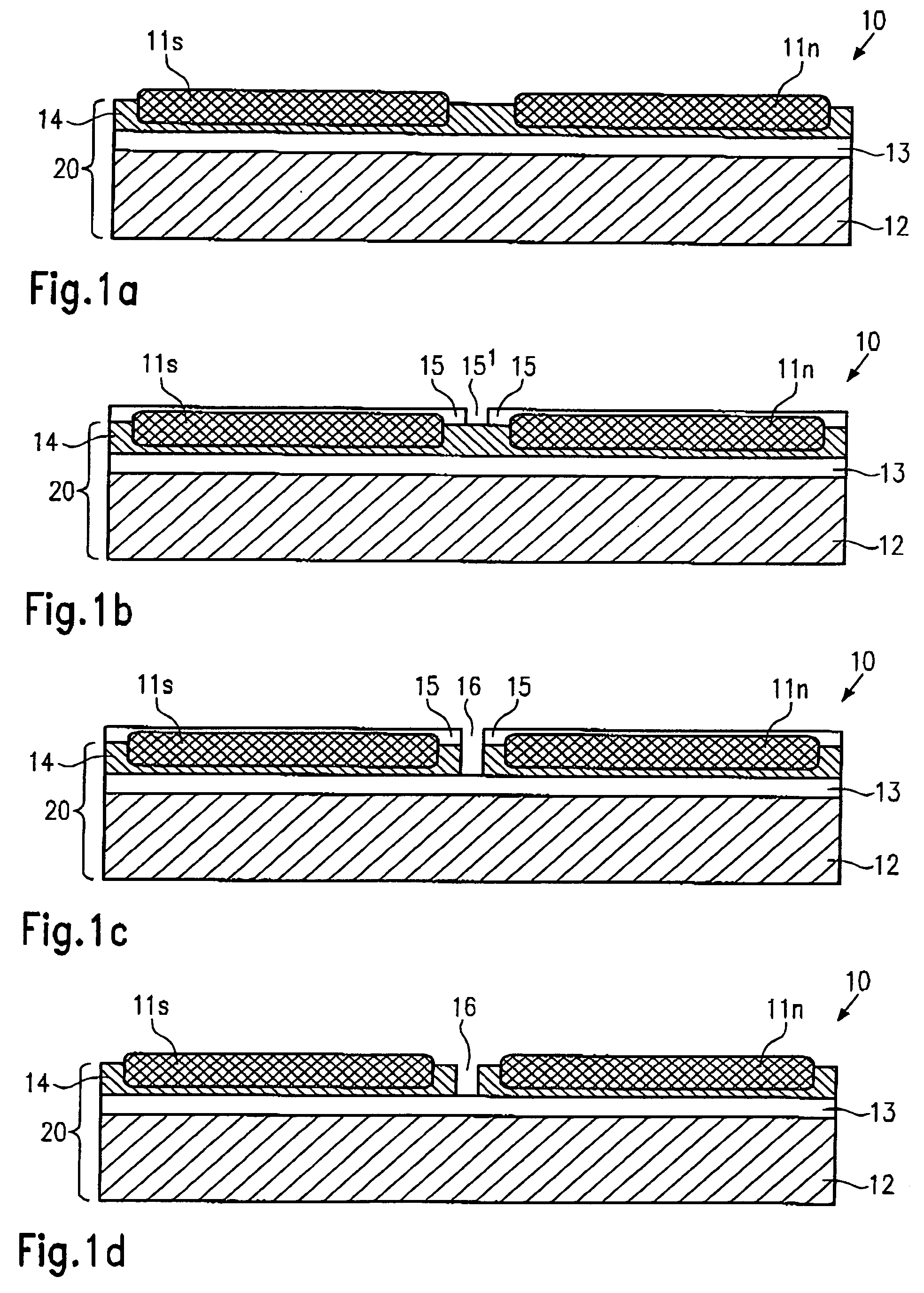
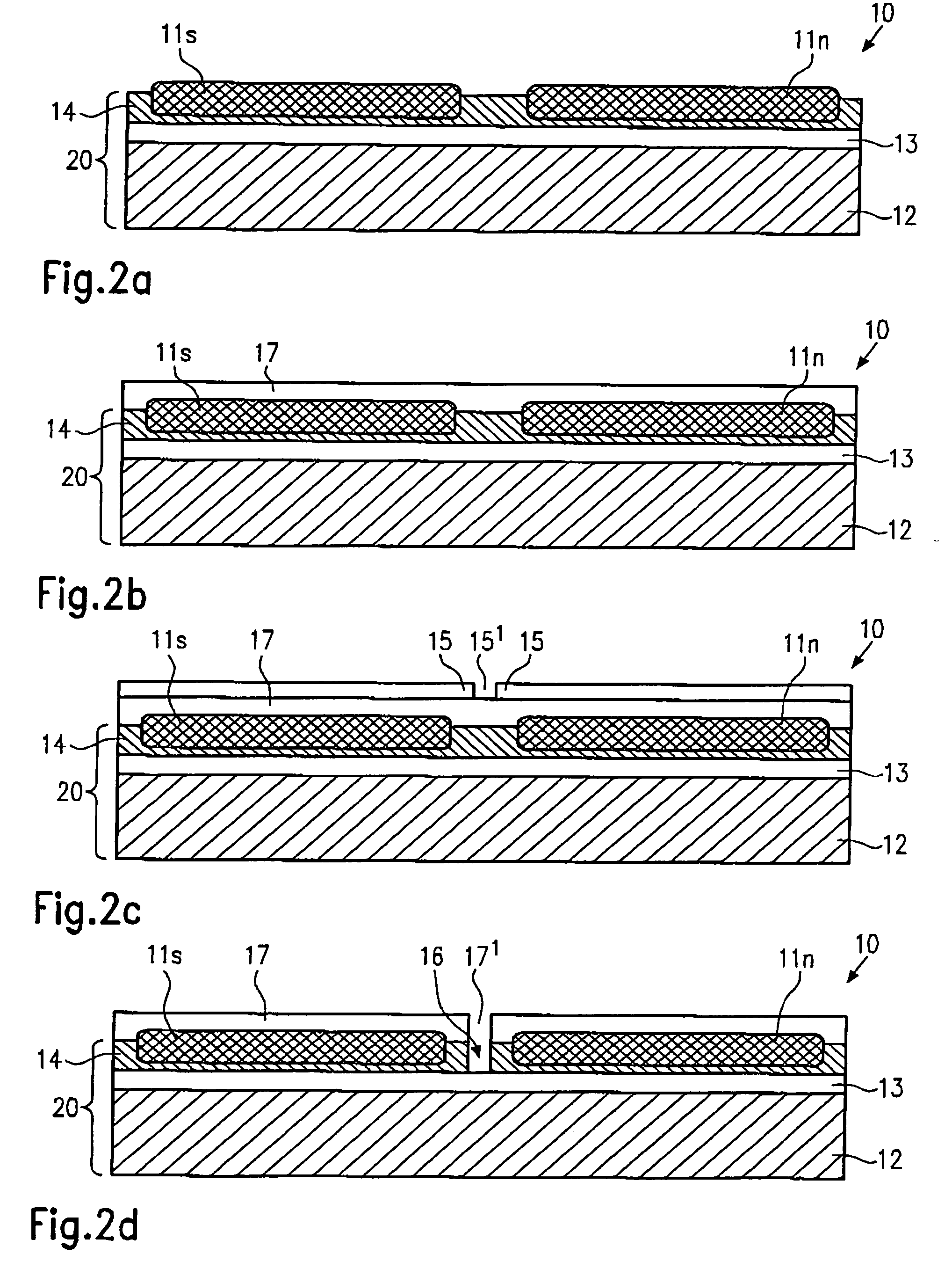
parasitic capacitance but requiring a very thin active silicon layer and very expensive manufacturing processes) circuits may be fabricated on “non-standard” SOI wafers, namely SOI wafers wherein the active silicon layer has a thickness substantially corresponding to the thickness of a standard bulk silicon layer of the kind used for standard CMOS and / or BiCMOS manufacturing technologies; portions of the circuits can then be separated from each other by removing portions of the thick active silicon layer between those portions of the circuits to be separated, thus reducing crosstalk interference between these circuit portions. Accordingly, expensive manufacturing processes and / or expensive substrates (such as SOI wafers with a very thin active silicon layer) can be avoided but benefit can be taken of the advantages offered by low cost manufacturing technologies, such as bulk CMOS and / or BiCMOS manufacturing technologies.
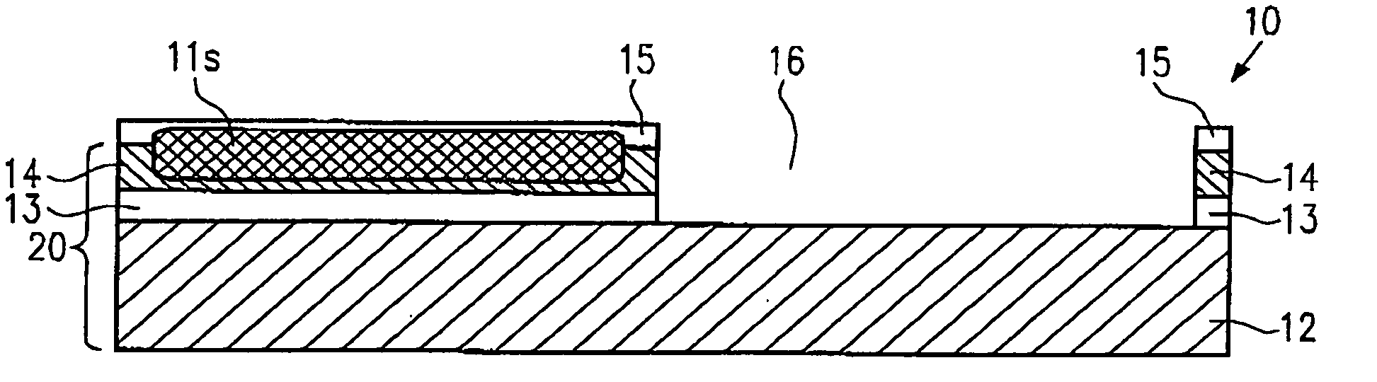
[0015] According to another embodiment, the present invention relates to a method of disposing at least one circuit on a substrate, wherein said method comprises providing a substrate comprising at least an upper layer of a semiconductive material with a first predefined thickness and a layer of dielectric material with a second predefined thickness below said layer of semiconductive material. The method further comprises providing at least two portions of said at least one circuit on said substrate, wherein at least one portion of said at least one circuit is provided on said layer of semiconductive material and forming at least one trench on said substrate at least as deep as said first predefined thickness so as to reduce interferences between at least one portion and at least one other portion of said circuit.
[0016] According to still another embodiment, the present invention relates to a circuit on a substrate, wherein said substrate comprises an upper layer of a semiconductive material with a first predefined thickness and a layer of a dielectric material with a second predefined thickness below said layer of semiconductive material. Said circuit further comprises at least two portions, with at least one portion being provided on said layer of a semiconductive material and said substrate comprises at least one trench at least as deep as said first predefined thickness so as to reduce interferences between at least one first portion and at least one other portion of said circuit.
[0017] The present invention has been revealed to be particularly advantageous for those applications where analog-mix mode signal circuits and digital switching circuits have to be monolithically integrated. In particular, the present invention is particularly advantageous in the case of optical transceivers, where transmitters such as laser diode drivers, digital control circuits or the like, and receivers such as highly sensitive trans-impedance amplifiers, limiting amplifiers and clock recovery circuits or the like, have to be monolithically integrated on the same substrate and during the same manufacturing process. Moreover, very relevant advantages are also obtained in those applications where active and / or passive optic (for example Planar Lightwave Circuits) and Optoelectronics Circuitry have to be monolithically integrated; for instance, said Planar Lightwave Circuits may comprise V-grooves for fiber interface, etched mirrors for receiver photodiodes as well as etched areas for laser coupling to the waveguide; the Optoelectronics Circuitry may comprise transimpedance amplifiers, liming amplifiers and / or clock / data recovery, laser diode drivers, analog RF video amplifier. Very high performances in term of reduced crosstalk interference were also obtained in those applications in which both sensitive and noisy circuits are provided on a thick SOI wafer (namely an SOI wafer comprising a thick upper active silicon layer) according to standard CMOS and / or BiCMOS manufacturing technologies.

Problems solved by technology

However, with ever decreasing feature sizes, the integration on the same chip of components performing differing functions (for instance transmitters and receivers) has been revealed as being a very challenging task.
In fact, the performance of a chip or unit comprising different components such as, for example noisy and sensitive components, are strongly affected by the crosstalk interferences arising between these components.
However, for central processing units (CPU) operating at clock frequencies of up to 1 GHz and above, the prior art solutions usually adopted in combination with standard bulk CMOS and / or BiCMOS manufacturing processes (triple well, guard rings or the like) have revealed to be not satisfactory, since the isolation between the circuit components obtained by means of these solutions is not sufficient and the performances of the chip are still negatively affected by crosstalk interference arising between these components, in particular between adjacent components.
However, fabricating semiconductor devices on SOI wafers has several drawbacks.
SOI technology is a high cost technology; in particular, this is due to the fact that when SOI wafers are used, processes have to be carried out which are much more expensive than the processes carried out for fabricating semiconductor circuits starting from usual bulk silicon layers.
Moreover, SOI wafers are much more expensive than standard bulk silicon layers; in particular, fabricating CMOS circuits on SOI wafers in conformity with SOI fabrication techniques requires that the active silicon layer be thinner than 50 nm.
Finally, transistors on SOI wafers are affected from the floating body effect; in fact, the lower silicon layer is isolated by the intermediate dielectric layer and cannot be easily connected to the front side of the wafer.
However, at least one electrical contact to the lower silicon layer has to be provided since a floating layer under the sandwiched dielectric layer may have an unpredictable impact on the devices fabricated on the wafer during operation.

Method used


Image

  • SOI circuit having reduced crosstalk interference and a method for forming the same
  • SOI circuit having reduced crosstalk interference and a method for forming the same
  • SOI circuit having reduced crosstalk interference and a method for forming the same

Examples


Embodiment Construction

[0024] While the present invention is described with reference to the embodiments as illustrated in the following detailed description as well as in the drawings, it should be understood that the following detailed description as well as the drawings are not intended to limit the present invention to the particular illustrative embodiments disclosed, but rather the described illustrative embodiments merely exemplify the various aspects of the present invention, the scope of which is defined by the appended claims.

[0025] As stated above, the present invention is understood to be particularly advantageous when used for providing circuits or portions thereof on SOI wafers, wherein said SOI wafers comprise an upper active semiconductive layer with a thickness substantially corresponding to the thickness of standard bulk semiconductive layers of the kind used for manufacturing integrated circuits according to standard processes. For this reason, example will be given in the following in...


PUM


Abstract

A method allowing the elimination of crosstalk interference, through the semiconductive substrate, between portions of a circuit provided on a same substrate comprising an upper semiconductive layer and an underlying dielectric layer, for instance an SOI wafer, wherein said portions are separated one from each other by forming trenches on said substrate either down to the dielectric layer or, in the case of an SOI substrate, down to the lower semiconductive layer.

Description

CROSS REFERENCE TO RELATED APPLICATION [0001] This application claims priority under 35 U.S.C. §§119 and / or 365 to Application Serial No. EP 04 008 436.0 filed in the European Community on Apr. 7, 2004, the entire disclosure of which is hereby incorporated by reference. FIELD OF THE PRESENT INVENTION [0002] The present invention relates to the field of fabrication of integrated circuits, and particularly to the field of fabrication of silicon on insulator (SOI) circuits; in more detail, the present invention relates to a method allowing to reduce and / or eliminate crosstalk interferences between different portions of integrated circuits fabricated on SOI wafers. BACKGROUND [0003] The need for high performance semiconductor chips has continued to increase over the past several years while, at the same time, the amount of area of the chip has decreased. Moreover, in modern integrated circuits, components having different functions need to be integrated on the same chip; for instance, d...

Claims


Application Information

Patent Timeline
Patent Type & Authority Applications(United States)
IPC IPC(8): H01L21/00H01L21/762H01L21/84H01L27/115H01L27/12
CPCH01L21/76224H01L27/1203H01L27/11502H01L21/84H10B53/00
Inventor PIZZARULLI, ANDREA
Owner PIZZARULLI ANDREA
Why Eureka
Try Eureka