

Bimetal layer manufacturing method
a manufacturing method and metal layer technology, applied in the direction of capacitors, semiconductor devices, electrical equipment, etc., can solve the problems of circuit transmission speed decline, parasitic capacitor phenomenon becomes more severe, rc delay is even more serious, etc., to reduce rc delay on the circuit, improve product quality, and increase element speed
- Summary
- Abstract
- Description
- Claims
- Application Information
AI Technical Summary
Benefits of technology
Problems solved by technology
Method used
Image

Examples
embodiments
[0022] The bimetal layer manufacturing method according to the invention includes the procedure as follow:
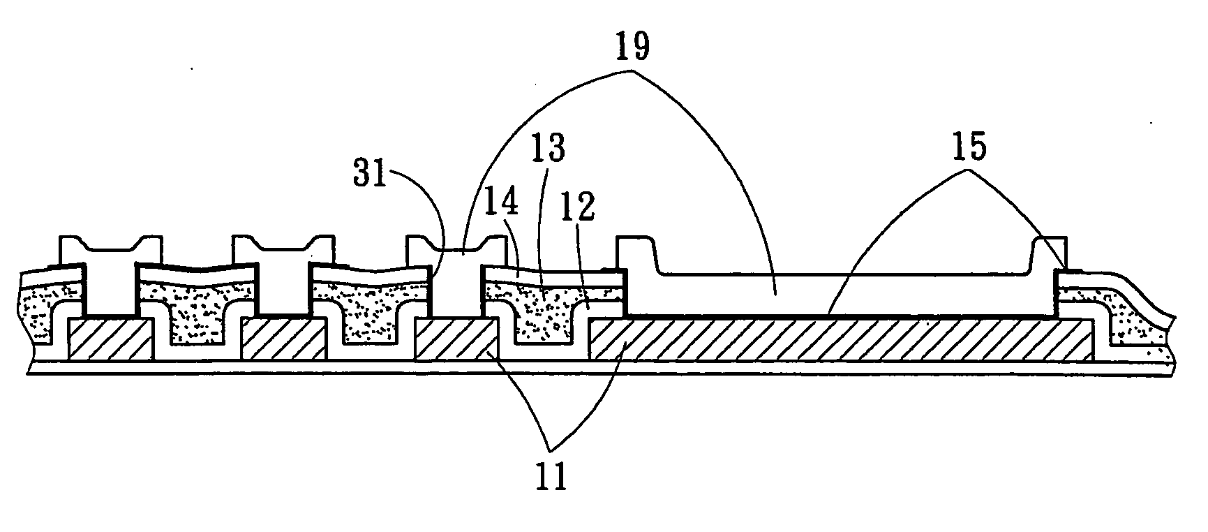
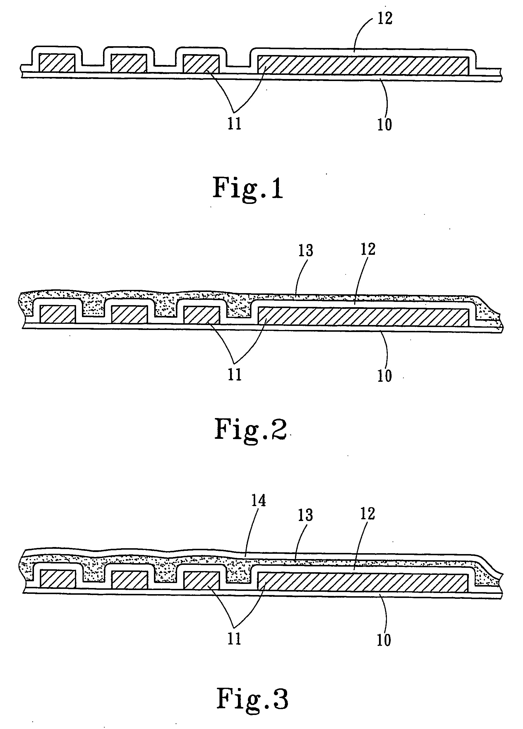
[0023] a. Provide a semiconductor substrate 10 which has a first metal layer 11 of a selected pattern formed thereon, and form a first dielectric layer 12 to cover the surfaces of the first metal layer 11 and the substrate 10 as shown in FIG. 1. The first metal layer 11 is selected from the group consisting of aluminum, copper, aluminum copper alloy, and aluminum copper and silicon alloy.
[0024] b. Form a SOG layer 13 on the surface of the first dielectric layer 12 to flatten the indented first dielectric layer 12 caused by the pattern of the first metal layer 11 as shown in FIG. 2. The first dielectric layer 12 is selected from the group consisting of silicon dioxide, silicon nitride, nitrogen silicon oxide, phosphor silicon glass, and boron phosphor silicon glass.
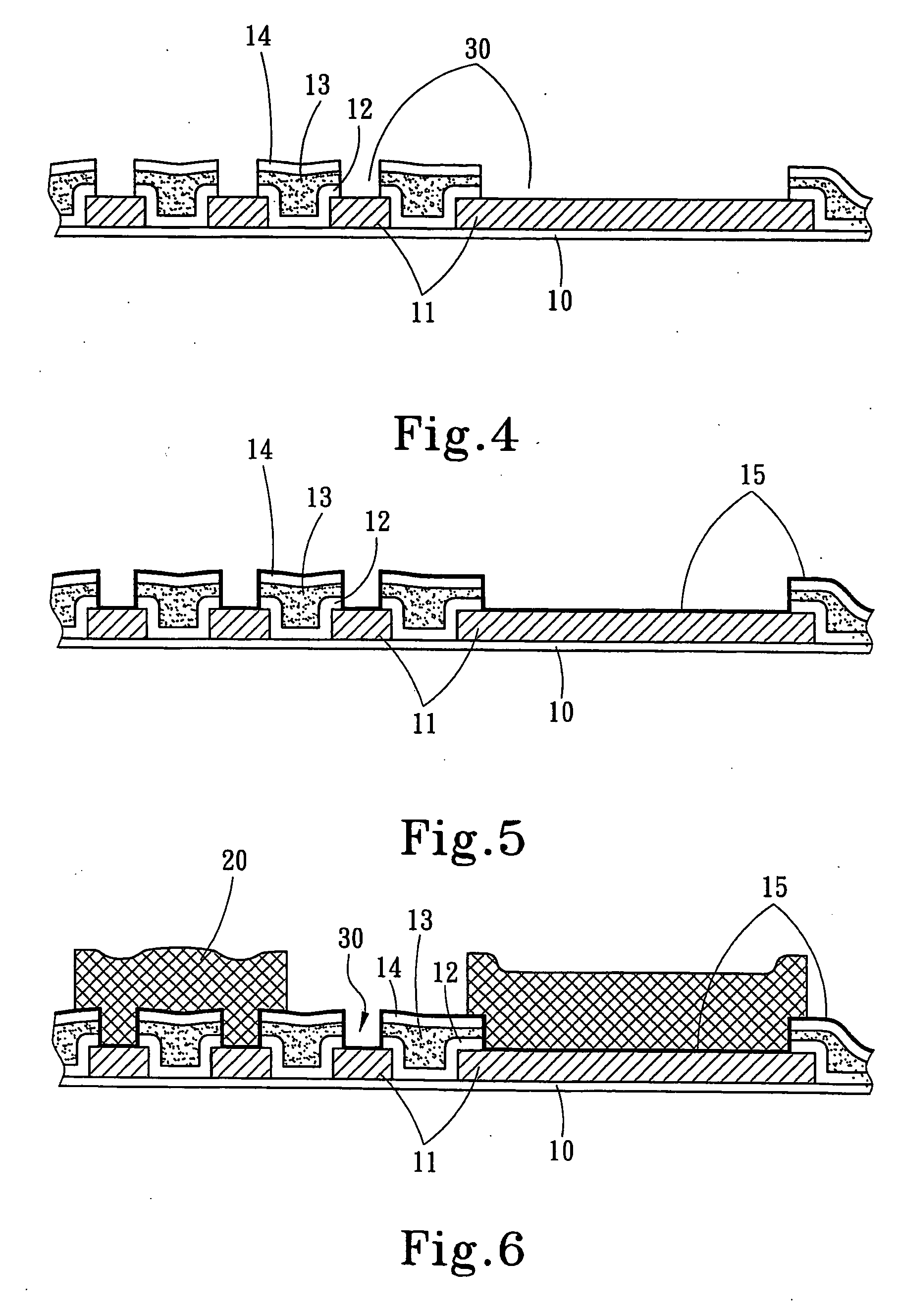
[0025] c. Form a second dielectric layer 14 as shown in FIG. 3. Then form required via holes 30 on the second die...
PUM
| Property | Measurement | Unit |
|---|---|---|
| dielectric constant | aaaaa | aaaaa |
| dielectric constant | aaaaa | aaaaa |
| dielectric | aaaaa | aaaaa |
Abstract
Description
Claims
Application Information