

Organic field effect transistor and method of manufacturing the same
a technology of organo-electric transistors and transistors, which is applied in the direction of thermoelectric device junction materials, semiconductor devices, electrical equipment, etc., can solve the problems of deterioration of the element characteristics, the gradual change of the fet characteristics or on/off ratio, and the insatiable on/off ratio of current between the source and the drain or improvement of the gate insulating film
- Summary
- Abstract
- Description
- Claims
- Application Information
AI Technical Summary
Benefits of technology
Problems solved by technology
Method used
Image

Examples
first embodiment
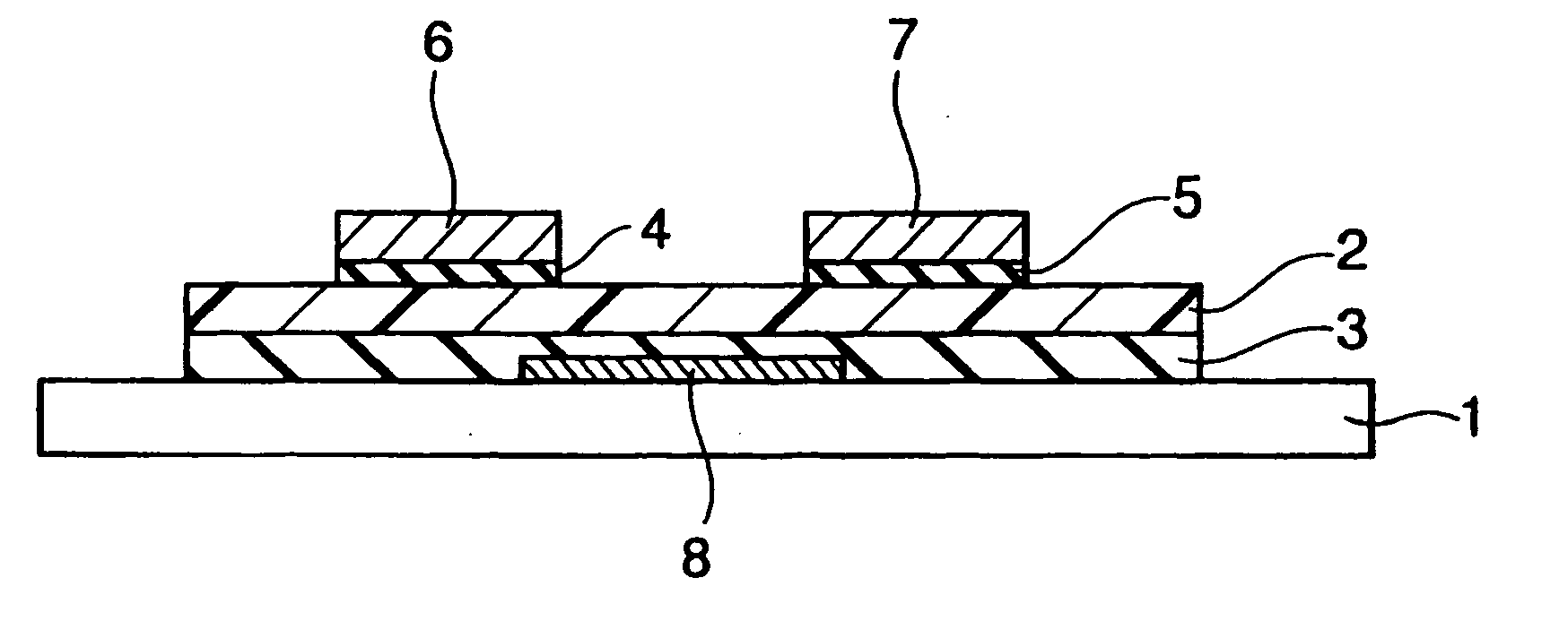
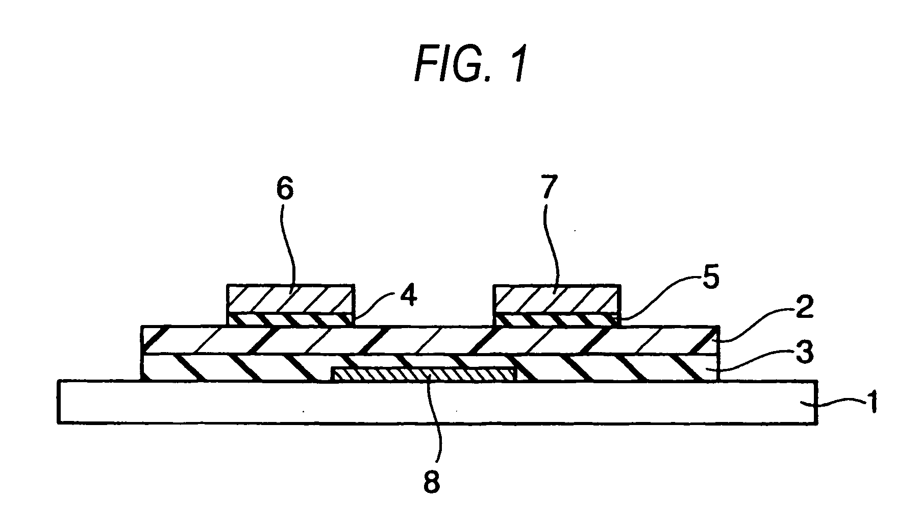
[0125] The present invention has the structure that at least one of a source electrode and a drain electrode come in contact with an organic semiconductor film made of an organic semiconductor material with a charge injection layer made of an inorganic material interposed to achieve stable element characteristics.
[0126]FIG. 1 shows the structure of an organic field effect transistor. It has the stack structure where source and drain electrodes 6 and 7 and a gate electrode 8 are formed so as to be opposite to each other with an organic semiconductor film 2 formed above a substrate 1 interposed. A source-side charge injection layer 4 and a drain-side charge injection layer 5 are formed between the source electrode 6 and the organic semiconductor film 2 and between the drain electrode 7 and the organic semiconductor film 2, respectively.
[0127] According to the invention having the above-mentioned structure, stable element characteristics can be achieved and an organic field effect tr...
example 1
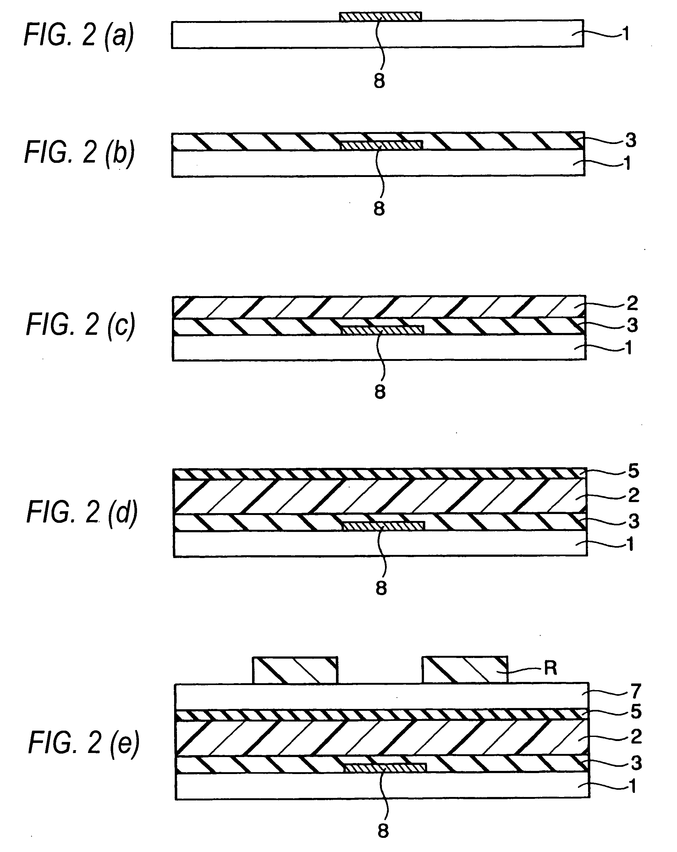
[0173] Next, a first example according to the present invention will be described below. First, an aluminum (Al) thin film is formed on a substrate 1 made of glass by about 500 nm thickness under 0.27 mPa (2×10⁻⁶ Torr) using a resistant heat deposition apparatus and then patterned using a photolithography method to form a gate electrode 8 (FIG. 2(a)).
[0174] Next, a polyimide film is deposited thereon to form a gate insulating film 3 (FIG. 2(b)), polyphenylenevinylene is spin coated thereon and then subject to a heat treatment to form a p-type organic semiconductor film 2 containing polyphenylenevinylene as a main component (FIG. 2(c)).
[0175] Next, the sample is divided into two samples. A source-side charge injection layer 4 and a drain-side charge injection layer 5 are formed on one sample (hereinafter, referred to as a present sample) and not formed on the other sample (hereinafter, referred to as a comparative sample).
[0176] On the present sample, as shown in FIG. 2(d), as the...
second embodiment
[0181] Next, a second embodiment according to the present invention will be described below. According to the first embodiment, the source-side charge injection layer 4 and the drain-side charge injection layer 5 have the same patterns as the source electrode 6 and the drain electrode 7, respectively. However, the second embodiment, as shown in FIG. 4, has a structure where the source-side charge injection layer 14 and the drain-side charge injection layer 15 are integrally formed as a charge injection layer 14S formed to cover the entire surface of the organic semiconductor film 12. For the operation thereof, similar to the first embodiment, the charge injection effect can be obtained between the organic semiconductor film 12 and the source and drain electrodes 16 and 17. However, since the charge injection layer 14S covers the entire surface of the organic semiconductor film 12, air is prevented from permeating into the organic semiconductor film vulnerable to moisture and heat, t...
PUM
 Abstract
Description
Claims
Application Information