Anisotropic conductivity connector, conductive paste composition, probe member, and wafer inspection device, and wafer inspecting method

a technology of anisotropic conductivity and connector, which is applied in the direction of semiconductor/solid-state device testing/measurement, semiconductor/solid-state device details, instruments, etc., to achieve good conductivity and good conductivity

Inactive Publication Date: 2005-12-01
ISC CO LTD
View PDF3 Cites 22 Cited by
  • Summary
  • Abstract
  • Description
  • Claims
  • Application Information

AI Technical Summary

Benefits of technology

[0031] The present invention has been made on the basis of the foregoing circumstances and has as its first object the provision of an anisotropically conductive connector that good conductivity is surely achieved as to all conductive parts for connection, and insulating property between adjacent conductive parts for connection is surely achieved even when the pitch of electrodes as objects of connection is small, and good conductivity is retained over a long period of time even when it is used repeatedly under a high-temperature environment.

Problems solved by technology

However, the anisotropically conductive elastomer sheet is flexible and easy to be deformed, and so it is low in handling property.
Therefore, the positioning and the holding and fixing of the uneven distribution type anisotropically conductive elastomer sheet are going to be difficult upon its electrical connection to electrodes to be inspected of the object of inspection.
In the burn-in test on the other hand, there is a problem that even when the necessary positioning, and holding and fixing of the uneven distribution type anisotropically conductive elastomer sheet to an integrated circuit device has been realized once, positional deviation between conductive parts of the uneven distribution type anisotropically conductive elastomer sheet and electrodes to be inspected of the integrated circuit device occurs when they are subjected to thermal hysteresis by temperature change, since coefficient of thermal expansion is greatly different between a material (for example, silicon) making up the integrated circuit device that is the object of inspection, and a material (for example, silicone rubber) making up the uneven distribution type anisotropically conductive elastomer sheet, as a result, the electrically connected state is changed, and thus the stably connected state is not retained.
In a burn-in test on the other hand, it takes a long time to individually conduct electrical inspection of a great number of integrated circuit devices because each integrated circuit device that is an object of inspection is fine, and its handling is inconvenient, whereby inspection cost becomes considerably high.
When a wafer that is an object of inspection is of large size of, for example, at least 8 inches in diameter, and the number of electrodes to be inspected formed thereon is, for example, at least 5,000, particularly at least 10,000, however, the following problems are involved when the above-described anisotropically conductive connector is applied as a probe member for the probe test or WLBI test, since a pitch between electrodes to be inspected in each integrated circuit is extremely small.
However, such an anisotropically conductive elastomer sheet is large in the whole area, but each conductive part is fine, and the area proportion of the surfaces of the conductive parts to the whole surface of the anisotropically conductive elastomer sheet is low.
It is therefore extremely difficult to surely produce such an anisotropically conductive elastomer sheet.
Since the conductive parts to be formed are fine, and the pitch thereof is extremely small, it is difficult to surely produce an anisotropically conductive elastomer sheet having necessary insulating property between adjacent conductive parts.
As a result, it is difficult to sufficiently ensure the insulating property between these conductive parts.
However, the use of such conductive particles involves the following problems.
Since the total sum of contact resistance among the conductive particles in one conductive path increases as a consequence, it is difficult to form conductive parts having high conductivity.
In addition, when a magnetic field is applied to the molding material layer for obtaining the anisotropically conductive elastomer sheet, the conductive particles become harder to move as the particle diameter thereof becomes smaller, so that the conductive particles remain in a great amount at portions to become the insulating parts in the molding material layer.
After all, it is difficult to sufficiently ensure the insulating property between the conductive parts.
At the same time, it is difficult to form conductive parts having expected conductivity because the conductive particles are not sufficiently gathered at the portions to become the conductive parts.
However, when the anisotropically conductive elastomer sheet is used repeatedly under such severe conditions, the ferromagnetic substance making up the core particles in the conductive particles migrates into the high-conductive metal forming the coating layer, so that the conductivity of the conductive particles at the surfaces thereof is deteriorated.
As described above, when the conductive particles having a small particle diameter are used, the conductivity of the conductive particles at the surfaces thereof is deteriorated, and the total sum of contact resistance among the conductive particles in the conductive paths formed markedly increases when the anisotropically conductive elastomer sheet is used repeatedly under the high-temperature environment, so that it is impossible to retain the necessary conductivity.
When a great difference is created between the wafer and the anisotropically conductive elastomer sheet in the absolute quantity of thermal expansion in a plane direction as described above, it is extremely difficult to prevent positional deviation between electrodes to be inspected in the wafer and the conductive parts in the anisotropically conductive elastomer sheet upon the WLBI test even when the peripheral edge of the anisotropically conductive elastomer sheet is fixed by a frame plate having an equivalent coefficient of linear thermal expansion to the coefficient of linear thermal expansion of the wafer.
However, in the means that the peripheral portions of the anisotropically conductive elastomer sheet are fixed by the screws or the like, it is extremely difficult to prevent positional deviation between the electrodes to be inspected in the wafer and the conductive parts in the anisotropically conductive elastomer sheet for the same reasons as the means of fixing to the frame plate as described above.
Since the anisotropically conductive elastomer sheet used in the WLBI test is small in the arrangement pitch of the conductive parts, and a clearance between adjacent conductive parts is small, however, it is extremely difficult in fact to do so.
In the means of fixing with the adhesive also, it is impossible to replace only the anisotropically conductive elastomer sheet with a new one when the anisotropically conductive elastomer sheet suffers from trouble, and so it is necessary to replace the whole probe member including the circuit board for inspection.
As a result, increase in inspection cost is incurred.

Method used


Image

  • Anisotropic conductivity connector, conductive paste composition, probe member, and wafer inspection device, and wafer inspecting method
  • Anisotropic conductivity connector, conductive paste composition, probe member, and wafer inspection device, and wafer inspecting method
  • Anisotropic conductivity connector, conductive paste composition, probe member, and wafer inspection device, and wafer inspecting method

Examples


example 1

(1) Frame Plate:

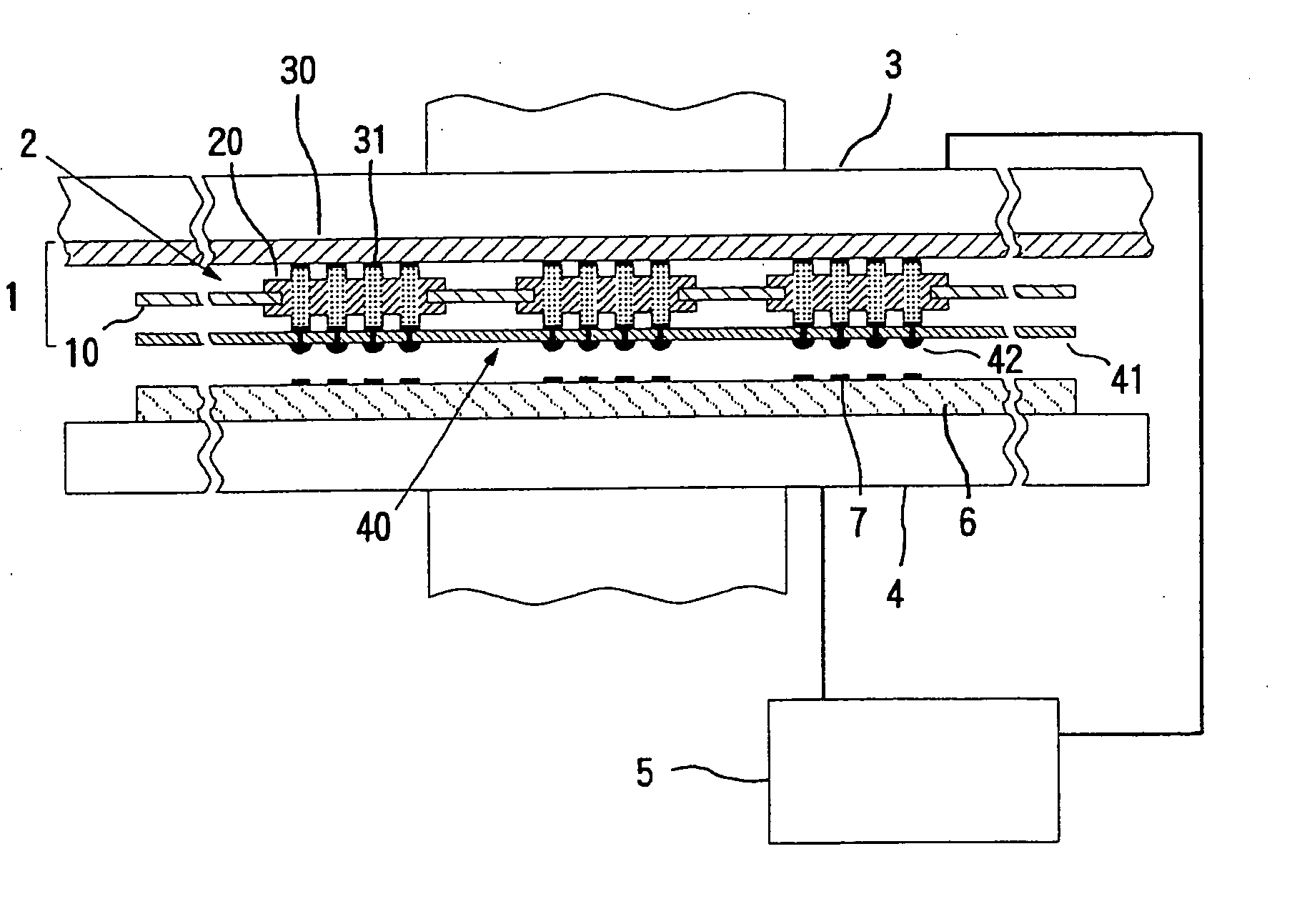
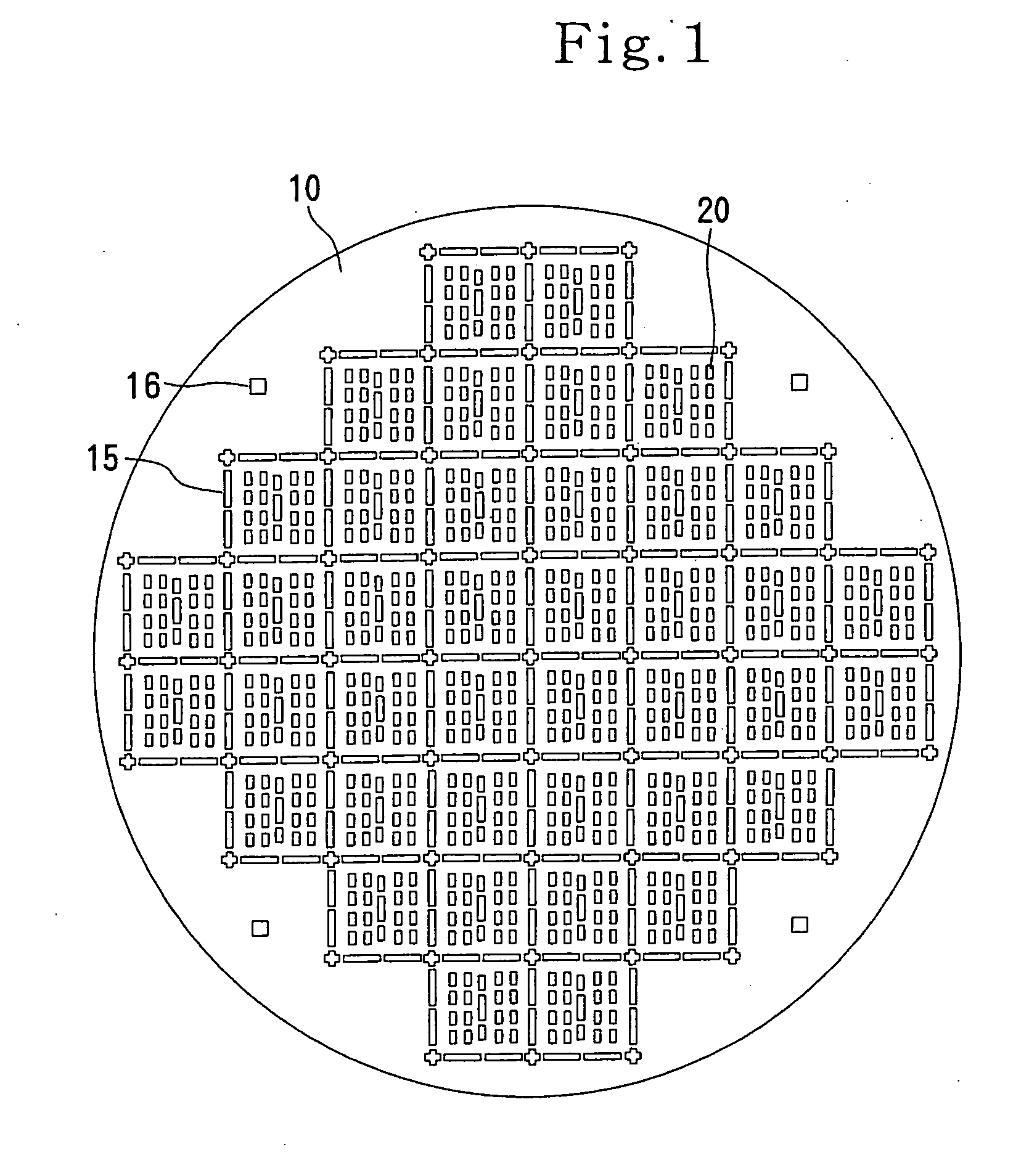
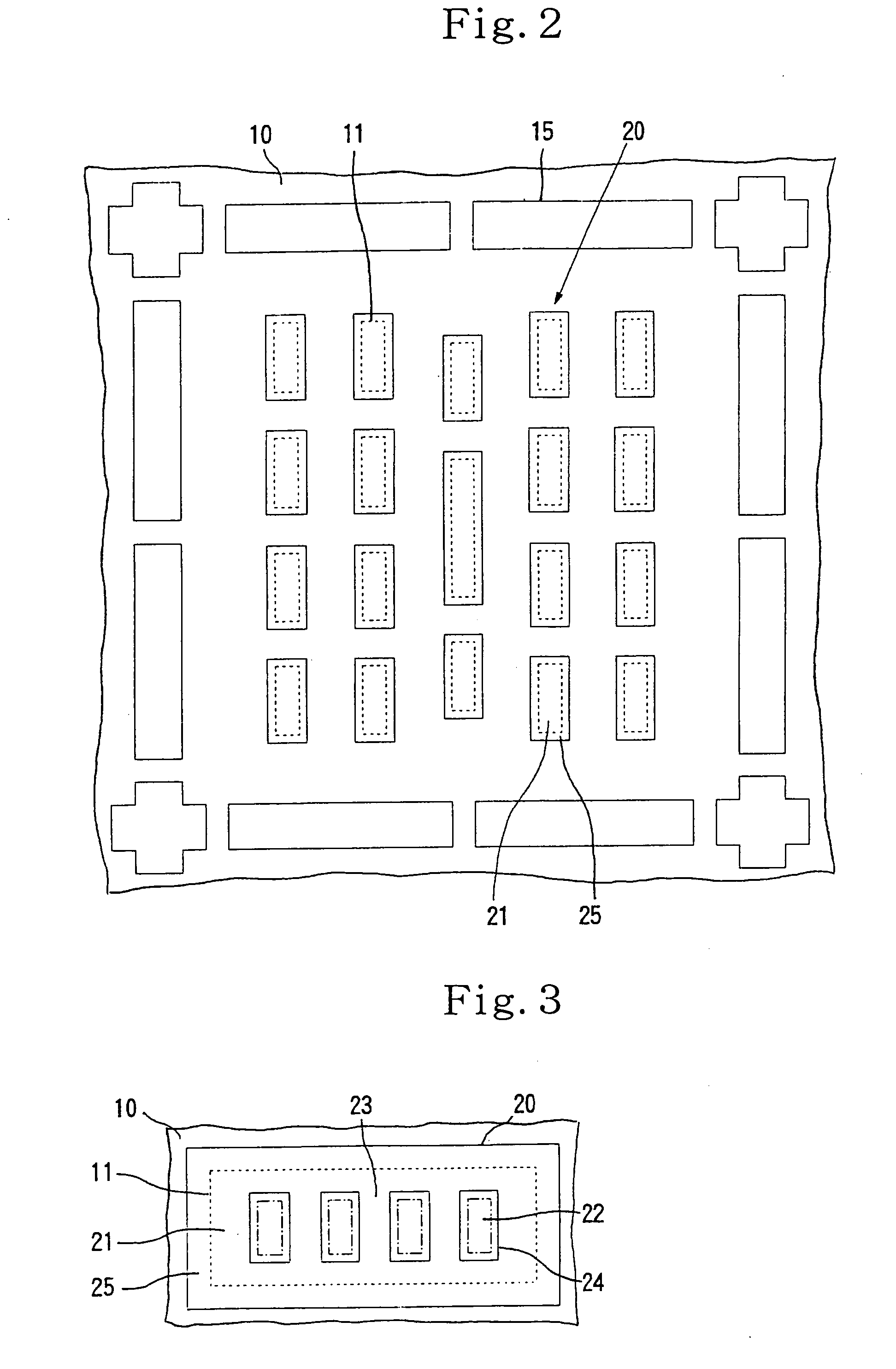
[0293] A frame plate having a diameter of 8 inches and 596 anisotropically conductive film-arranging holes formed correspondingly to the respective regions of the electrodes to be inspected in Wafer W for test described above was produced under the following conditions in accordance with the construction shown in FIGS. 19 and 20.

[0294] A material of this frame plate is covar (saturation magnetization: 1.4 Wb / m2; coefficient of linear thermal expansion: 5×10⁻⁶ / K), and the thickness thereof is 60 μm.

[0295] The anisotropically conductive film-arranging holes 11 each have dimensions of 1,540 μm in a lateral direction (left and right direction in FIGS. 19 and 20) and 600 μm in a vertical direction (upper and lower direction in FIGS. 19 and 20).

[0296] A circular air circulating hole 15 is formed at a central position between anisotropically conductive film-arranging holes 11 adjacent in the vertical direction, and the diameter thereof is 1,000 μm.

(2) Spacer:

[0297] ...

example 2

[0330] An anisotropically conductive connector was produced in the same manner as in Example 1 except that Conductive Particles (2) were used in place of Conductive Particles (1). This anisotropically conductive connector will hereinafter be referred to as “Anisotropically Conductive Connector C2”. In this Anisotropically Conductive Connector C2, the value of a ratio W / Dn of the shortest width W of the conductive part for connection to the number average particle diameter Dn of Conductive Particles (2) is 6.0.

[0331] The content of the conductive particles in the conductive parts for connection in each of the elastic anisotropically conductive films of Anisotropically Conductive Connector C2 thus obtained was investigated. As a result, the content was about 30% in terms of a volume fraction in all the conductive parts for connection.

[0332] The parts to be supported and the insulating parts in the functional parts of the elastic anisotropically conductive films were observed. As a r...

example 3

[0334] An anisotropically conductive connector was produced in the same manner as in Example 1 except that Conductive Particles (3) were used in place of Conductive Particles (1). This anisotropically conductive connector will hereinafter be referred to as “Anisotropically Conductive Connector C3”. In this Anisotropically Conductive Connector C3, the value of a ratio W / Dn of the shortest width W of the conductive part for connection to the number average particle diameter Dn of Conductive Particles (3) is 6.5.

[0335] The content of the conductive particles in the conductive parts for connection in each of the elastic anisotropically conductive films of Anisotropically Conductive Connector C3 thus obtained was investigated. As a result, the content was about 30% in terms of a volume fraction in all the conductive parts for connection.

[0336] The parts to be supported and the insulating parts in the functional parts of the elastic anisotropically conductive films were observed. As a r...


PUM

PropertyMeasurementUnit
number average particle diameteraaaaaaaaaa
diameteraaaaaaaaaa
diameteraaaaaaaaaa

Abstract

Disclosed herein are an anisotropically conductive connector that conductivity of all conductive parts for connection is good, and insulating property between adjacent conductive parts for connection is surely achieved even when the pitch of electrodes as objects of connection is small, and good conductivity is retained over a long period of time even when it is used repeatedly under a high-temperature environment, and applications thereof. The above anisotropically conductive connector is a connector having an elastic anisotropically conductive film, in which a plurality of conductive parts for connection containing conductive particles and extending in a thickness-wise direction of the film have been formed, wherein supposing that the shortest width of each of the conductive parts for connection is W, and the number average particle diameter of the conductive particles is Dn, a value of a ratio W/Dn of the shortest width of the conductive part for connection to the number average particle diameter of the conductive particles falls within a range of 3 to 8, and a coefficient of variation of particle diameter of the conductive particles is at most 50%.

Description

TECHNICAL FIELD [0001] The present invention relates to an anisotropically conductive connector suitable for use in conducting electrical inspection of a plurality of integrated circuits formed on a wafer in a state of the wafer, a conductive paste composition for obtaining this anisotropically conductive connector, a probe member equipped with this anisotropically conductive connector, a wafer inspection apparatus equipped with this probe member, and a wafer inspection method using this probe member, and particularly to an anisotropically conductive connector suitable for use in conducting electrical inspection of integrated circuits, which are formed on a wafer, a diameter of which is, for example, 8 inches or greater and a total number of electrodes to be inspected in the integrated circuits formed thereon is at least 5,000, in a state of the wafer, a conductive paste composition for obtaining this anisotropically conductive connector, a probe member equipped with this anisotropi...

Claims


Application Information

Patent Timeline
Patent Type & Authority Applications(United States)
IPC IPC(8): C09C3/06C09C1/62C09D5/24C09D183/04G01R1/06G01R1/073H01B1/00H01B1/22H01B5/16H01L21/66H01L23/498H01R11/01
CPCG01R1/07314G01R1/0735H01L23/49827H01L23/49866H01L2924/0002H01L2924/00H01R11/01G01R1/06H01L22/00H01B1/22
Inventor SETAKA, RYOJI
Owner ISC CO LTD
Why Eureka
Try Eureka