Electrostatic actuator formed by a semiconductor manufacturing process

a manufacturing process and actuator technology, applied in the direction of electrostatic generator/motor, mechanical vibration separation, instruments, etc., can solve the problems of low yield rate, difficult to accurately form such a small air gap with little, electrode deformation, etc., and achieve stable performance and less variation in characteristics

Inactive Publication Date: 2005-12-01
RICOH KK
View PDF10 Cites 28 Cited by
  • Summary
  • Abstract
  • Description
  • Claims
  • Application Information

AI Technical Summary

Benefits of technology

[0038] According to the above-mentioned invention, since the air gap between the vibration plate and the electrode is formed by etching the sacrifice layer, the distance between the vibration layer and the electrode can be accurately set to the thickness of the sacrifice layer. Additionally, the partition parts defining the air gap between the vibration plate and the electrode are formed by the remaining parts of the sacrifice layer after forming the air gap by etching, an upper surface of the vibration plate can be made flat. Thus, the electrostatic actuator according to the present invention is formed by a semiconductor manufacturing process, which results in a stable performance with less variation in characteristics.

Problems solved by technology

An electrostatic attraction force is generated between the pair of electrodes by applying a voltage across the electrodes (between the vibration plate and electrode), which results in deformation of the electrode (vibration plate).
However, in the head disclosed in the above-mentioned Japanese Laid-Open Patent Application No. 6-71882, since the air gap is formed by formation of a cavity by etching and bonding a vibration plate substrate by anode junction, it is very difficult to accurately form such a small air gap with little variation, which causes a problem that the yield rate is low.
Thus, in the head disclosed in the above-mentioned Japanese Laid-Open Patent Application No. 2001-18383, although the air gap is formed with sufficient accuracy in accordance with a gap-forming method using etching of the sacrifice layer, there is a problem in that a reliability of the vibration plate is low since etching holes for etching the sacrifice layer are formed in the vibration plate.
Thus, there is a problem in that the rigidity of the vibration plate increases and a drive voltage increases, which causes a fluctuation in the rigidity of the vibration plate.
Further, there is unevenness in the surface of the actuator substrate due to the formation of the air gap, and high alignment accuracy is required when joining a liquid chamber substrate.
Moreover, since the junction area is small, it tends to cause a work mistake such as destruction due to a contact at the time of joining etc., and there is also a problem that a reliability is decreased and the yield rate is decreased.
However, a problem tends to occur that an ink component is subjected to condensation since a voltage is applied to the ink in the gap, and there is a problem in that a high-speed drive cannot be performed due to the conductance of the ink in the gap.
Moreover, the above-mentioned Japanese Laid-Open Patent Application No. 9-193375 and Japanese Laid-Open Patent Application No. 2001-277505 do not disclose any method of forming a nonparallel air gap or any specific method for varying the thickness of the dielectric insulating layer, and, thus, a problem that it is very difficult to form a small air gap with little variation is not solved.
In the electrostatic inkjet head, the dimensional accuracy of a distance between the vibration plate and the electrode greatly affects the performance of the electrostatic inkjet head.
However, if the sacrifice layer removal holes are sealed by such a film deposition method, the components of the film may enter the air gap.
Additionally, the sacrifice layer removal holes also serve to maintain a strength of the partition wall, and they cannot be made small.
Therefore, the sacrifice layer removal holes being sealed by the film deposition using a PVD or CVD method may influence the operation characteristic and reliability of the actuator and it cannot deal with densification.
Moreover, since the thin vibration plate is floated on the surrounding parts after the sacrifice layer is removed, the vibration plate may be damaged in the subsequent process and it is difficult to manufacture the actuator with a sufficient yield rate.
Additionally, although the sacrifice layer removal holes are sealed by a film formed by a film deposition method using a vacuum device, the use of the vacuum device may cause a problem.
Therefore, there is a problem in that the vibration plate may be bent due to a negative pressure inside the air gap when the actuator is exposed to an atmosphere.
Additionally, if there is variation in the bent of the vibration plate, there may occur variation in the displacement of the vibration plate.
In addition, since the vacuum seal cannot provide a damping effect of a gas sealed in the air gap, variation in amplitude of vibration with respect to variation in the thickness of the vibration plate becomes large.
In order to solve such a problem, it is necessary to provide a structure or a process for opening the air to the atmosphere, which causes an increase in the cost and deterioration in the yield rate.
Thus, if the conventional sacrifice layer process is used, it is difficult to obtain an electrostatic actuator having high-accuracy and reliability at a low cost.
Especially, if a flow passage formation member is formed of silicon, silicon is eluted in ink and is deposited on a nozzle part, which causes degradation of image quality due to nozzle clogging or deterioration of coloring of ink.
If the material of the component parts is changed to solve the problem, it is difficult to realize high-density processing or processing accuracy may be deteriorated in many cases.
Moreover, the change in the material requires a large change in the fabrication process or assembly process, which results in decrease of nozzle density and consequently causing degradation of the print quality.
Since the organic resin film such as paraxylene is formed by the vacuum vapor deposition method, the covering characteristic of the film is not good due to its nature of deposition, and a large unevenness arises in the distribution of film thickness inside the liquid chamber or on the vibration plate.
When an area where the film thickness is small contacts with ink for a long time, there is a large problem arises in the long-time reliability since the corrosion resistant film is dissolved and finally the base material is subjected to corrosion.
Moreover, a large bend is generated due to a distribution of internal stresses caused by variation of film thickness of the organic resin film on the vibration plate, which causes a large variation in the ink injection characteristic.
Moreover, in the head in which a metallic ink resistant film is formed on the vibration plate by a sputtering method or a vapor deposition method, the covering characteristic of the corrosion resistant film is poor similar to the above-mentioned organic resin film.
Therefore, a long-time reliability cannot be obtained, and further a large bent is generated in the vibration plate due to fluctuation in the thickness of the metallic ink-resistant film, which causes variation in the ink injection characteristic.
Especially, this problem is serious in the electrostatic head rather than the piezoelectric head since the distance between the vibration plate and the electrode varies due to the vibration plate being bent and the drive voltage differing from the design value.
Further, in the head in which the above-mentioned corrosion resistant film is formed, the reliability of operation is low such that the vibration plate contacts the electrode due to an influence of an external environment such as humidity since the air gap between the vibration plate and the electrode is not sealed.
Moreover, in the head in which the air gap between the vibration plate and the electrode is sealed so as not to receive an influence from an external environment, there is a restriction of pH value of ink that is usable since the corrosion resistant film is not formed on the vibration plate, and, thus, matching with ink must be maintained and a cost is increased.

Method used


Image

  • Electrostatic actuator formed by a semiconductor manufacturing process
  • Electrostatic actuator formed by a semiconductor manufacturing process
  • Electrostatic actuator formed by a semiconductor manufacturing process

Examples


first embodiment

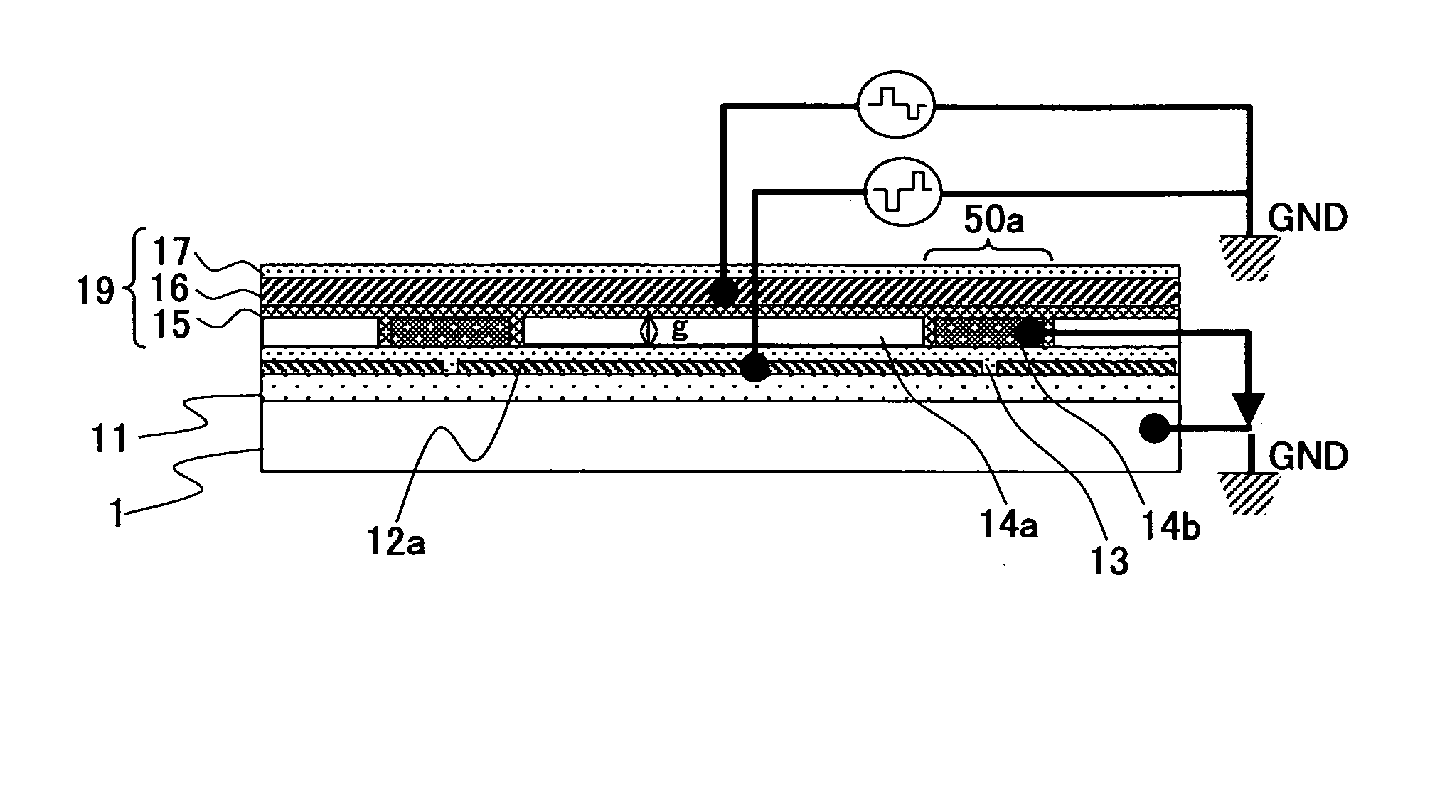
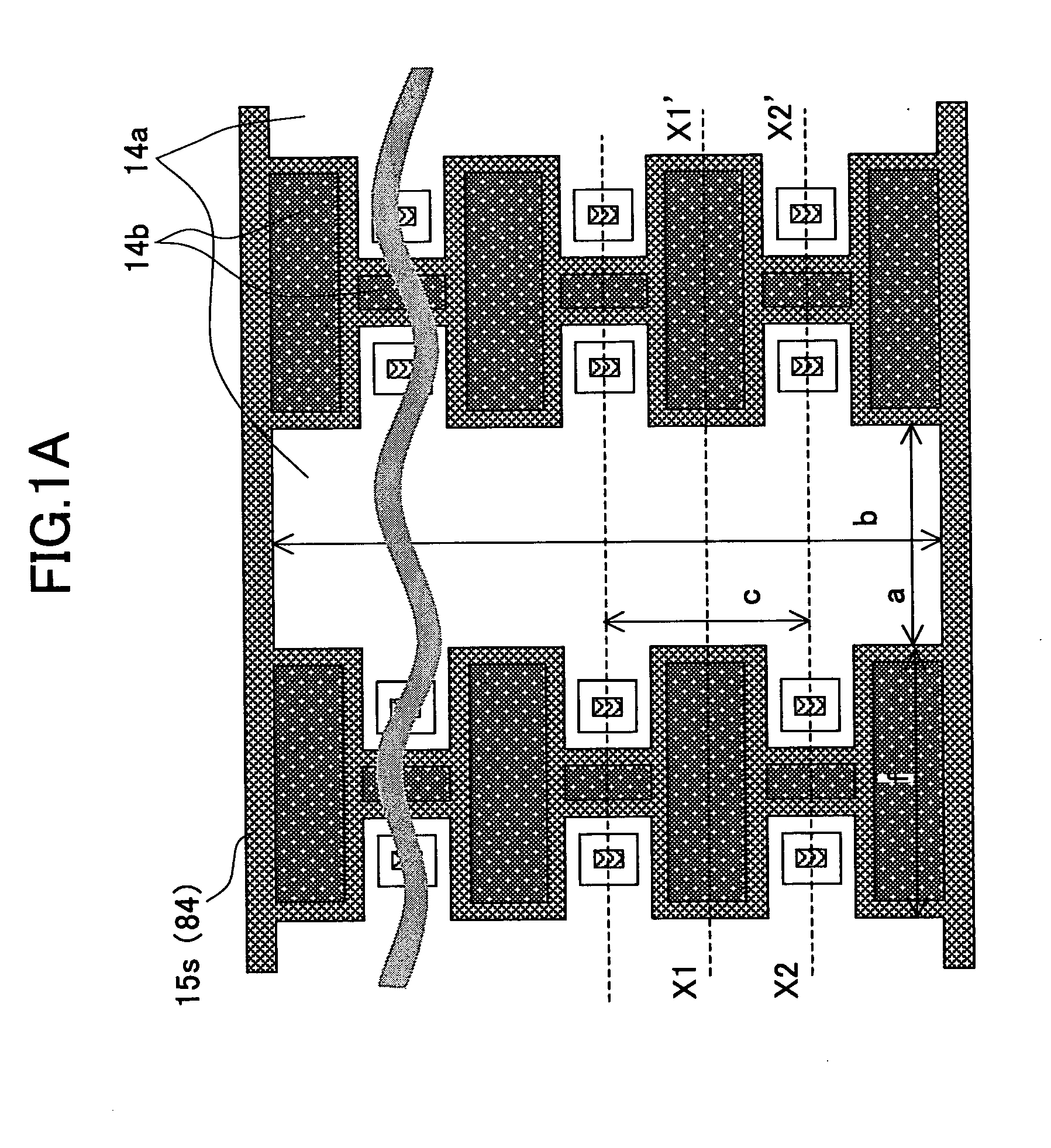
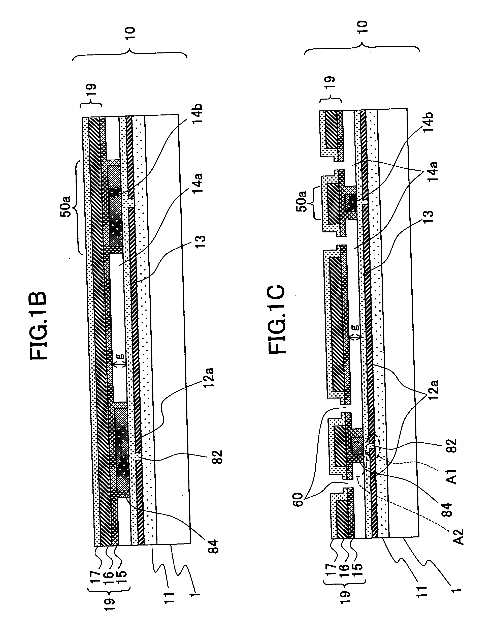
[0110] A description will now be given, with reference to FIGS. 1A, 1B and 1C and FIGS. 2A, 2B and 2C, of a first embodiment of the present invention. FIG. 1A is a plan view of the electrostatic actuator according to a first embodiment of the present invention. FIGS. 1B and 1C show cross-sectional views (two parallel cross sections) taken along a line X1-X1′ and a line X2-X2′ in FIG. 1A, respectively.

[0111] In the figures, 1 denotes a substrate which forms an actuator; 11 an insulating layer; 12a an electrode (may be referred to as individual electrode); 14 a sacrifice layer; 15 an insulating layer (may be referred to as a vibration plate side insulating layer); 16 a vibration plate electrode layer; and 17 an insulating layer which also serves as a stress-adjustment of a vibration plate. Additionally, 19 denotes a vibration plate constituted by the insulating layer 15, the vibration plate electrode layer 16 and the insulating layer 17. Further, 14a denotes an air gap formed by remo...

second embodiment

[0128] A description will now be given, with reference to FIGS. 3A and 3B, FIG. 4 and FIGS. 5A and 5B, of a second embodiment of the present invention. In FIGS. 3A and 3B, FIG. 4 and FIGS. 5A and 5B, parts that are the same as the parts shown in FIGS. 1B and 1C are given the same reference numerals.

[0129] In the figures, 1 denotes a substrate which forms an actuator; 11 an insulating layer; 12a an electrode (may be referred to as individual electrode); 12b a dummy electrode; 14 a sacrifice layer; 15 an insulating layer (may be referred to as a vibration plate side insulating layer); 16 a vibration plate electrode layer; and 17 an insulating layer which also serves as a stress-adjustment of a vibration plate. Additionally, 19 denotes a vibration plate constituted by the insulating layer 15, the vibration plate electrode layer 16 and the insulating layer 17. Further, 14a denotes an air gap formed by removing a part of the sacrifice layer; “g” a distance of the air gap; 60 a sacrifice...

third embodiment

[0155] A description will now be given, with reference to FIGS. 6A through 6E, of an actuator according to a third embodiment of the present invention. FIG. 6A is a perspective plan view of an electrostatic actuator according to the third embodiment of the present invention. FIG. 6B is a cross-sectional view taken along a line X1-X1′ of FIG. 6A. FIG. 6C is a cross-sectional view taken along a line X2-X2′ of FIG. 6A. FIG. 6D is a cross-sectional view taken along a line Y1-Y1′ of FIG. 6A. FIG. 6E is a cross-sectional view taken along a line Y2-Y2′ of FIG. 6A.

[0156] In the figures, the reference numeral 1 denotes a substrate for forming the actuator; 11 an insulating layer; 12a an electrode (may be referred to as an individual electrode); 12b a dummy electrode; 13 an insulating layer (may be referred to as an electrode side insulating layer); 14 a sacrifice layer; 15 an insulating layer (may be referred to as a vibration plate side insulating layer); 16 a vibration plate electrode lay...


PUM


Abstract

An electrostatic actuator has high-reliability and less variation in characteristics. An electrode (12a) is formed on a substrate (1), and a plurality of partition parts (50a) are formed on the electrode. A vibration plate (19) is formed on the partition parts (50a), and is deformable by an electrostatic force generated by a voltage applied to the electrode (12a) so that an air gap (14a) is formed between the partition parts (50a) by etching a part of a sacrifice layer (14) formed between the electrode (12a) and the vibration plate (19). The partition parts (50a) are formed of remaining parts of the sacrifice layer (14) after the etching.

Description

TECHNICAL FIELD [0001] The present invention relates to electrostatic actuators and, more particularly, to an electrostatic actuator used for a liquid-discharging mechanism such as an inkjet head of an inkjet recording apparatus. BACKGROUND ART [0002] An inkjet recording apparatus is used as an image recording apparatus or an image forming apparatus such as a printer, a facsimile machine, a copy machine, etc. An inkjet recording apparatus is equipped with an inkjet head as a droplet-discharging head. Generally, such an inkjet head comprises: a single or a plurality of nozzles for discharging droplets of ink; a discharge chamber connecting with the nozzles; and pressure generating means for generating a pressure to pressurize the ink in the discharge chamber. The discharge chamber may be referred to as a pressurizing chamber, an ink chamber, a liquid chamber, a pressurizing liquid chamber, a pressure chamber or an ink passage. Droplets of ink are discharged from the nozzles by pressu...

Claims


Application Information

Patent Timeline
Patent Type & Authority Applications(United States)
IPC IPC(8): B41J2/14B41J2/16
CPCB41J2/14314B41J2/16B41J2/1623B41J2/1628B41J2/1629B06B1/0292B41J2/1642B41J2/1645B41J2/1646B41J2002/14411B41J2/1639
Inventor NISHIMURA, MANABUKURODA, TAKAHIKOABE, SHUYATANAKA, MAKOTOIRINODA, MITSUGUHASHIMOTO, KENICHIROH
Owner RICOH KK
Why Eureka
Try Eureka