Semiconductor device, noise reduction method, and shield cover

a semiconductor and shield cover technology, applied in the direction of semiconductor/solid-state device details, earth/grounding circuits, instruments, etc., can solve the problems of unnecessarily radiating electromagnetic noise from the memory module, affecting the performance of the device, etc., to achieve the effect of low emi module, less radiation, and reducing unnecessary electromagnetic radiation

Inactive Publication Date: 2005-12-08
NEC CORP +2
View PDF12 Cites 15 Cited by
  • Summary
  • Abstract
  • Description
  • Claims
  • Application Information

AI Technical Summary

Benefits of technology

[0021] According to the above structure, since connection points to a reference potential are effectively disposed along the signal lines, feedback currents, to which the currents are fed back, flow through paths having short distances thereto (small loops) and near to the paths of signals. As a result, the magnetic fields formed by the feedback currents are cancelled each other, thereby electromagnetic waves are less radiated to the outside, and thus a low EMI module can be arranged.
[0022] In the present invention, since the potential of the metal protection cover (that is, the shield cover) can be set nearer to the reference potential, the shield cover and the substrate of the memory module are unlike to act as a patch type antenna, thereby unnecessary electromagnetic radiation can be reduced. Further, although the currents induced by the LSI operation flow in the metal cover, since the grounding points of shield cover are set such that the induction currents are dispersed and directed in the same direction as that of the control system signals, the unnecessary electromagnetic radiation resulting from the currents can be more reduced.

Problems solved by technology

Further, as the operating frequency of a memory module is also increased, a serious problem arises in that electromagnetic noises are unnecessarily radiated from the memory module.
However, since the semiconductor chips having such arrangement are less resistant to external stress and the like as well as require consideration to a heat dissipation effect.
However, the following problems still remain to effectively reinforce and electromagnetically shield the memory module having high density and high speed in correspondence to the recent computer technology.
First, in the technology disclosed in the above-mentioned patent document 1 in which the shield sheet is formed by laminating the adhesive sheet and the aluminum sheet and bonded on the upper surfaces of the memory chips and the upper surface of the printed circuit substrate so as to cover the semiconductor memory chips to thereby electromagnetically shield the memory chips as well as fix them to the printed circuit substrate, drawbacks arise in that distortion is liable to be caused by bonding due to the difference of the thermal expansion coefficients between the memory module and the shield sheet and that it is difficult to secure a heat dissipation property and a bonding surface area.
However, it is difficult to actually apply this connection to a product.
However, the ground pattern cannot be form on the circuit substrate around the entire periphery of the shield cover because signal lines are formed on the substrate.
Further, it is also difficult to cause the substrate to bring into contact with the entire periphery of the shield cover because of the structural problem of the shield cover.
Moreover, even if the substrate is forcibly caused to bring into contact with the entire periphery of the shield cover, distortion is caused by the difference of thermal expansion coefficients due to the increased contact area thereof.
Further, as apparent from the above description, since the mechanism of noises radiated from the memory module is obscure, an effective installation method is not apparent.

Method used


Image

  • Semiconductor device, noise reduction method, and shield cover
  • Semiconductor device, noise reduction method, and shield cover
  • Semiconductor device, noise reduction method, and shield cover

Examples


Embodiment Construction

[0033] Embodiments of the present invention will be described below in detail with reference to the drawings.

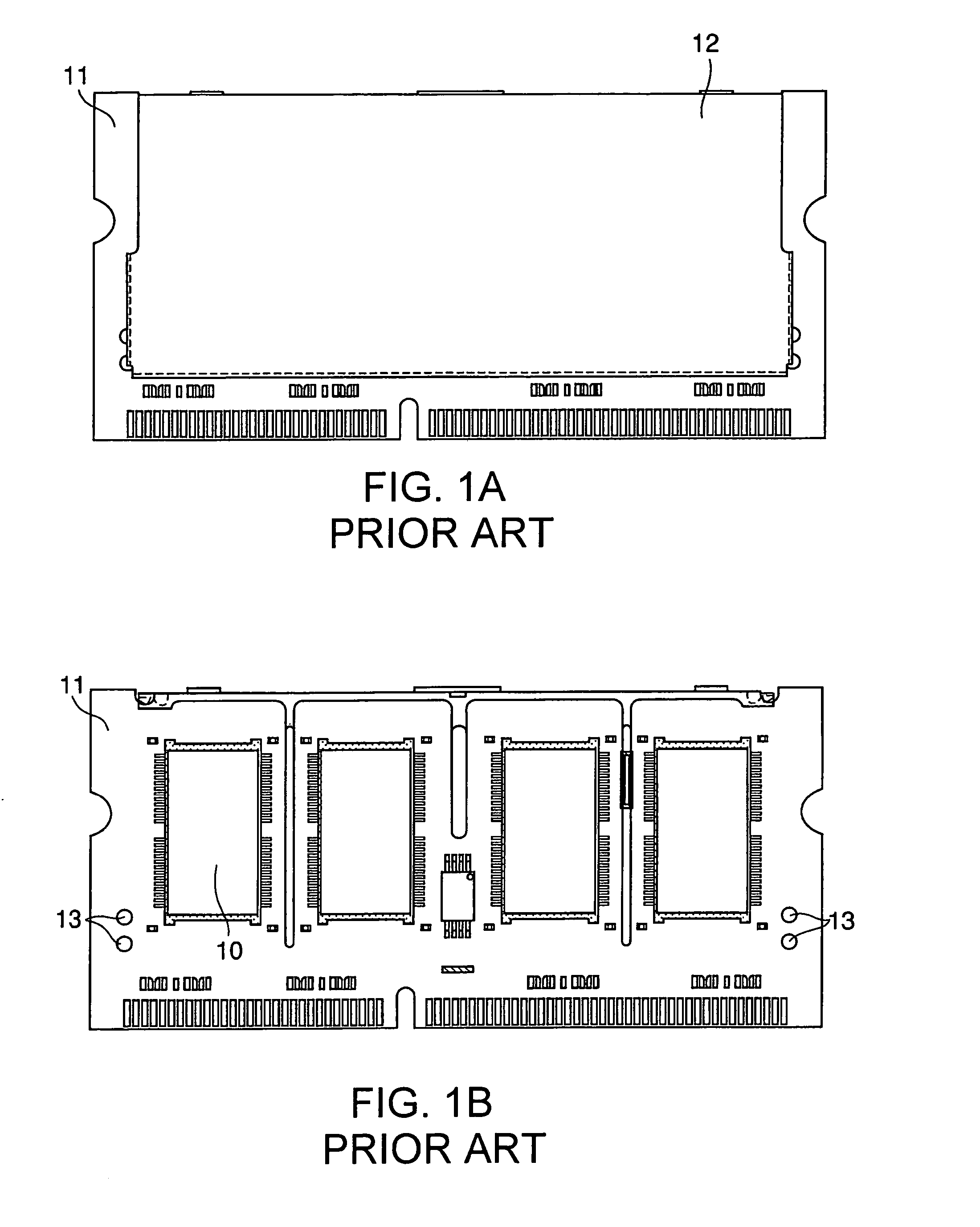
[0034]FIGS. 3A, 3B, and 3C show a memory module as an example of a semiconductor module according to an embodiment of the present invention.

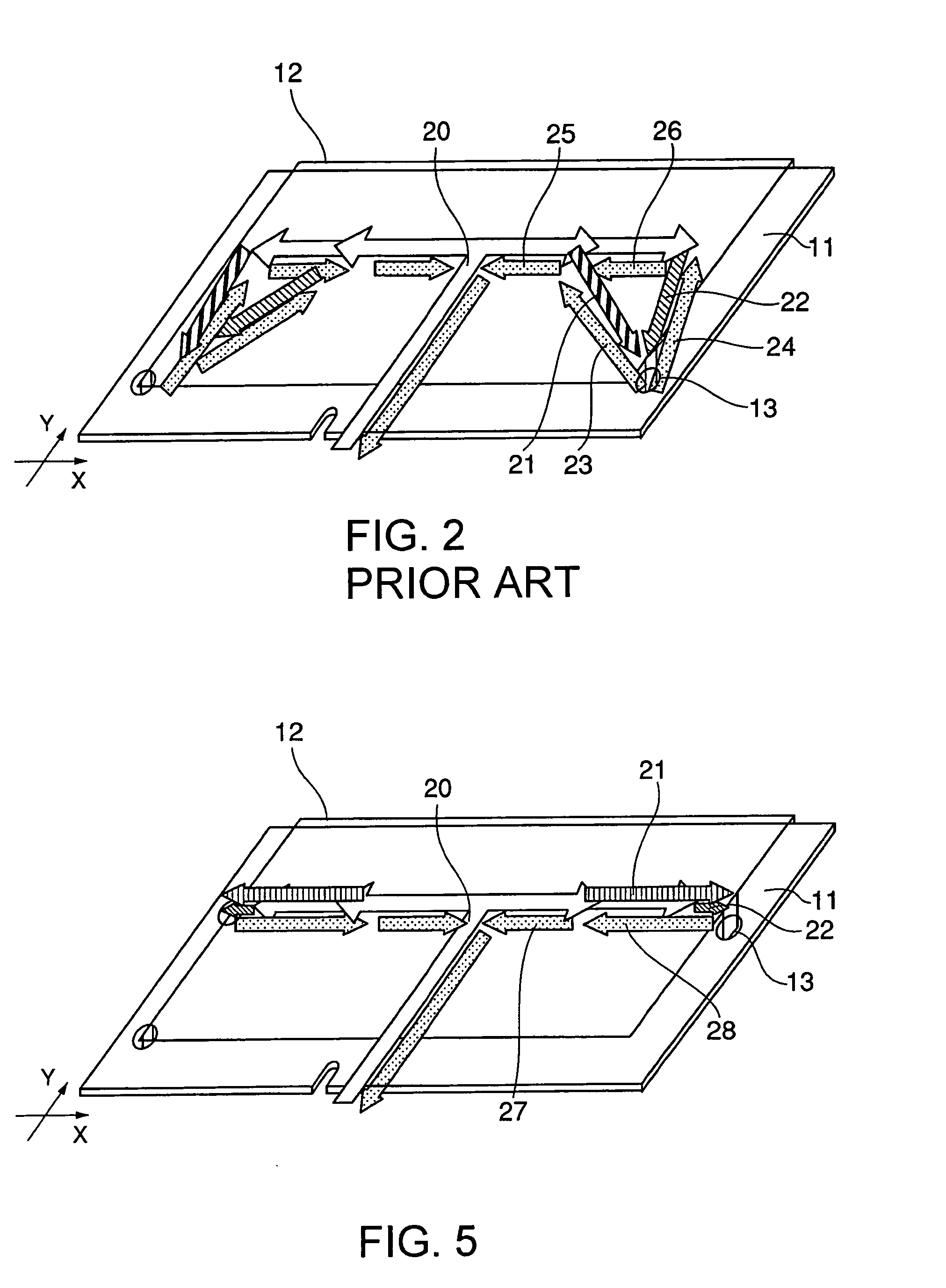
[0035]FIG. 3A is a plan view of the memory module of the present invention having a shield cover 12 with a conductive member mounted on a circuit substrate 11, and FIG. 3B is a plan view of the memory module of the present invention in which the shield cover 12 is removed from the circuit substrate 11. Further, FIG. 3C is a sectional view of a contact part 16 for electrically connecting the shield cover 12 of the present invention to a reference potential on the circuit substrate 11, and the contact part 16 constitutes a metal cover connection conductor.

[0036] As shown in FIGS. 3A and 3B, the memory module of the present invention includes the circuit substrate 11, a plurality of semiconductor memory chips 10 mounted on the circuit sub...


PUM


Abstract

In a memory module, reference potential connecting patterns are disposed on high frequency signal lines and/or on the extension lines extending from the terminal ends of the signal lines as well as a shield cover for covering semiconductor memory chips is disposed on the substrate, and the reference potential connecting patterns are connected to the shield cover through metal cover contact parts.

Description

[0001] This application claims priority to prior application JP 2004-150915, the disclosure of which is incorporated herein by reference. BACKGROUND OF THE INVENTION [0002] 1. Field of the Invention [0003] The present invention relates to semiconductor devices mounted on a memory module used in a computer apparatus and the like and on other multi-chip module, and the like, a method of reducing unnecessary radiation noises in the semiconductor device, and a shield cover used in the semiconductor device. [0004] 2. Description of the Related Art [0005] Recently, as the size of a notebook computer and the like is reduced in the field of a computer industry, a memory module as a semiconductor module used as a main memory is made more dense and smaller in size. The memory module is a memory device having semiconductor memory chips mounted thereon at high densities so that they operate at a high speed. The memory module is required to mount a larger number of memory chips in the limited mo...

Claims


Application Information

Patent Timeline
Patent Type & Authority Applications(United States)
IPC IPC(8): G11C5/00H05K9/00H01L23/00H05K1/02
CPCG11C5/04H05K1/0218H05K9/0064
Inventor IMAZATO, MASAHARUNAKAMURA, ATSUSHIWATANABE, TAKAYUKITSUNEDA, KENSUKEKATAGIRI, MITSUAKISHIMIZU, HIROYANAGATA, TATSUYA
Owner NEC CORP
Why Eureka
Try Eureka