Ultraviolet curing process for spin-on dielectric materials used in pre-metal and/or shallow trench isolation applications

a technology curing process, which is applied in the field of ultra-violet curing process of low-k dielectric film used in pre-metal and shallow trench isolation applications, can solve the problems of undetected exposure of the wafer to an elevated temperature for an extended period of time, and the temperature can exceed the allowable thermals budget of the manufacturer, so as to reduce the organic content of the dielectric material

Inactive Publication Date: 2005-12-08
AXCELIS TECHNOLOGIES
View PDF18 Cites 96 Cited by
  • Summary
  • Abstract
  • Description
  • Claims
  • Application Information

AI Technical Summary

Benefits of technology

[0006] Disclosed herein are processes for UV curing a spin-on pre-metal dielectric material coated onto a surface of a substrate. In one embodiment, a UV curing process for a dielectric material used in pre-metal and shallow tr

Problems solved by technology

Each of these approaches has some limitations for filling very narrow gaps that will need to be overcome for successful integration.
In either case, the conventional cure process undesirably subjects the wafer to an elevated temperature for an extended period of time (e.g., in excess of one hour to several hours and at a temperature in greater than about 300° C.).
These temperatures can exceed the allow

Method used


Image

  • Ultraviolet curing process for spin-on dielectric materials used in pre-metal and/or shallow trench isolation applications
  • Ultraviolet curing process for spin-on dielectric materials used in pre-metal and/or shallow trench isolation applications
  • Ultraviolet curing process for spin-on dielectric materials used in pre-metal and/or shallow trench isolation applications

Examples


example 1

Wet Etch Resistance of Pre-Metal Dielectric Material

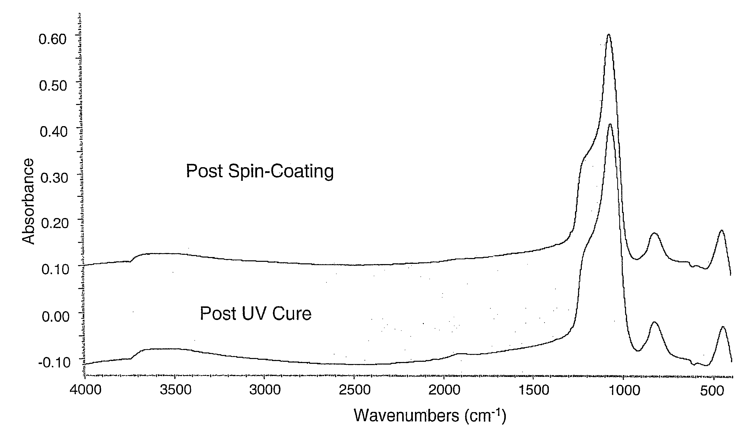
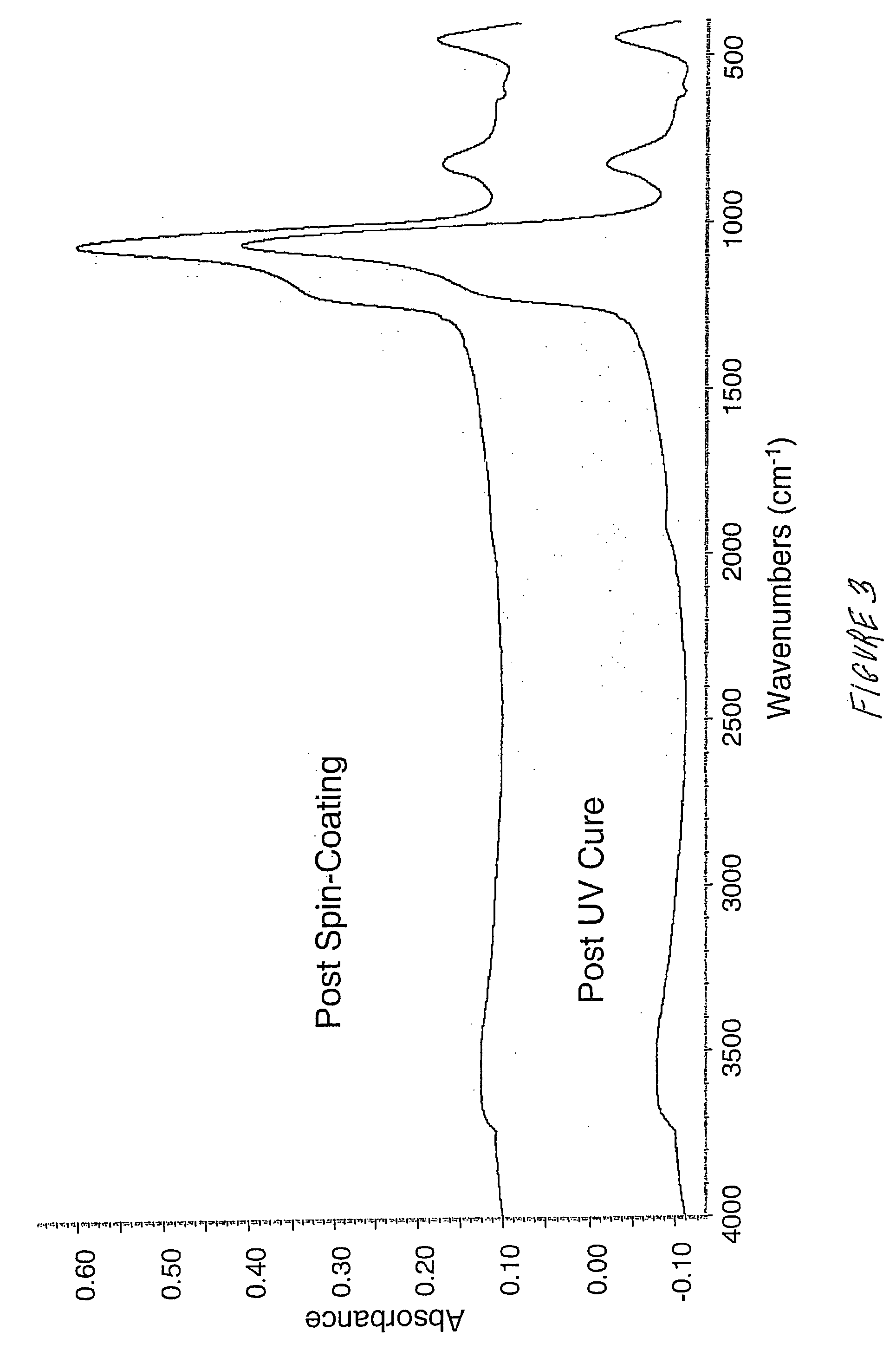
[0030] In this Example, a pre-metal dielectric material identified as Honeywell Electronic Material A (HEMA) and obtained from Honeywell Company was spin coated onto bare silicon wafers. The wafers were subjected to a conventional spin process recommended by the manufacturer. Each wafer was processed identically. The coated wafers were exposed to a UV cure process at 425° C. for a period of 5 minutes. The UV cure process employed various microwave electrodeless bulbs in a Rapid Cure Exposure tool commercially available from Axcelis Technologies, Incorporated. FTIR data as shown in FIG. 3 did not show any detectable absorbance changes in the low k dielectric material after the UV cure. The UV cured wafers were then exposed to a wet etching process that comprised immersing the wafers in a 40:1 and a 100:1 dilute hydrofluoric acid aqueous based solution for 2 minutes, 5 minutes, and 10 minutes. The above ratio represents the amount b...

example 2

Wet Etch Resistance of HEMA Based Spin-on Dielectric Material

[0032] In this example, the HEMA pre-metal spin-on dielectric material was spin coated onto blank wafers as in Example 1. In addition, a nanoglass spin on dielectric material available from the Honeywell Corporation under the identifier NGX was spin coated onto blank wafers. The wafers were exposed to UV radiation produced in the RapidCure tool utilizing a Type III electrodeless bulb at 425° C. for 10 minutes in an inert gas mixture. The thickness and the refractive index (RI) after the spin on dielectric was post baked and after the UV cure process were measured. Some of the wafers were further exposed to a furnace anneal process at 900° C. or 1000° C. for 1 hour. Percent shrinkage is calculated based on the thickness before and after UV cure process, and anneal, if applicable. In this Example, wafer set number 1 refers to the HEMA spin coated dielectric materials, and wafer set numbers 2 and 3 refer to the spin coated N...

example 3

[0035] In this Example, the dielectric constant and breakdown voltage was measured before and after the UV cure process as in Example 1. Spin low k dielectrics identified as HEMA (m1), (m2), and (m3) were coated using a conventional spin coat process as recommended by the manufacturer for the particular low k dielectric. The results are shown in Table 3 below.

TABLE 3HEMA (m1)HEMA (m2)HEMA (m3)PrePostPrePostPrePostUVUVUVUVUVUVCureCureCureCureCureCureDielectric7.846.916.276.197.66.7ConstantBreakdown0.581.881.992.041.242.27Voltage

[0036] In each instance, exposing the spin-on dielectric material to the UV cure process advantageously decreased the dielectric constant. Along with the decrease in dielectric constant a concomitant increase in breakdown voltage was observed.


PUM


Abstract

A UV curing process for a dielectric material used in pre-metal and shallow trench isolation applications comprises coating a suitable dielectric material onto a substrate; and exposing the dielectric material to ultraviolet radiation in an amount effective to reduce an organic content and/or increase a density and./or increase a wet etch resistance of the dielectric material. Optionally, the UV cured dielectric material may be exposed to multiple ultraviolet radiation patterns.

Description

CROSS REFERENCE TO RELATED APPLICATIONS [0001] This application relates to and claims priority to U.S. Provisional Application No. 60 / 577,679 filed on Jun. 7, 2004, incorporated herein by reference in its entirety.BACKGROUND [0002] The present disclosure generally relates to dielectric films in semiconductor devices, and more particularly, to ultraviolet (UV) curing processes for spin-on low k dielectric films used in pre-metal and shallow trench isolation applications. [0003] In the field of advanced semiconductor fabrication, the dimensions of the devices and spacings formed continue to be decreased so as to improve integrated circuit performance. Fabrication often requires the deposition of dielectric materials into features patterned into layers of material on silicon substrates. In most cases, it is important that the dielectric material completely fill such features without formation of any voids. Filling such narrow features, which is also referred to as gap filling, places s...

Claims


Application Information

Patent Timeline
IPC IPC(8): H01L21/20H01L21/31H01L21/3105H01L21/312H01L21/469H01L21/76
CPCH01L21/02126H01L21/02282H01L21/02337H01L21/02348H01L21/31058H01L21/3121H01L21/3122H01L21/3124H01L21/3125
Inventor WALDFRIED, CARLOESCORCIA, ORLANDO
Owner AXCELIS TECHNOLOGIES
Why Eureka
Try Eureka