
Structure and method of patterning a magnetic tunnel junction stack for a magneto-resistive random access memory

Active Publication Date: 2005-12-15
INFINEON TECH AG +1
View PDF38 Cites 61 Cited by
  • Summary
  • Abstract
  • Description
  • Claims
  • Application Information

AI Technical Summary

Benefits of technology

[0011] According to yet another aspect of the invention, a structure including a magnetic tunnel junction (MTJ) is provided. Such structure includes an MTJ stack having a first portion of a pinned layer, a first portion of a tunnel barrier layer overlying the first portion of the pinned layer, and a free layer overlying the first portion

Problems solved by technology

Flash memory, which utilizes thin dielectrics and is reprogrammed by applying relatively high voltage (10 V to 15 V) and current, typically fails within one million cycles.
The patterning of the MTJ device is one of the most challenging aspects of fabrication.
Conventional techniques used to pattern other structures of a chip, such as reactive ion etching (RIE) or ion milling, have been less than satisfactory when applied to the materials that compose magnetic stacks.
In most cases utilizing such techniques, it is extremely difficult to cleanly remove etched material.
Another problem of conventional etch techniques is corrosion and degradation of the patterned free and pinned layers that form the MTJ, due to chemical residue remaining after etching.
Exposure to reactive gases during deposition of dielectrics such as silicon nitride and silicon dioxide after the etching of the MTJ can also cause corrosion and degradation.
When subjected to high temperatures, the residue can migrate and cause corrosion, degradation and electrical shorting.
However, the tight process control and high selectivity required to maintain an acceptably controlled etch process across an entire wafer is difficult to achieve.
Moreover, the SOA process does not necessarily protect the free layer from harmful corrosion and degradation.

Method used


Image

  • Structure and method of patterning a magnetic tunnel junction stack for a magneto-resistive random access memory
  • Structure and method of patterning a magnetic tunnel junction stack for a magneto-resistive random access memory
  • Structure and method of patterning a magnetic tunnel junction stack for a magneto-resistive random access memory

Examples


Embodiment Construction

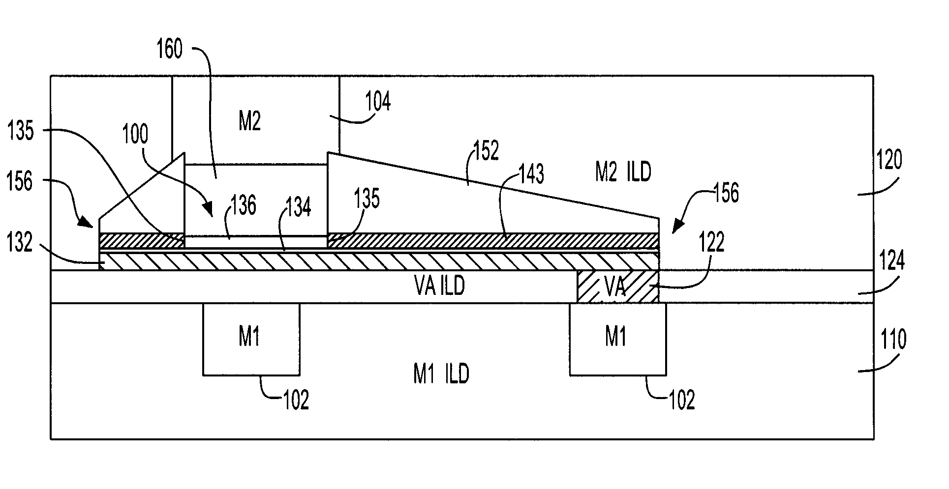
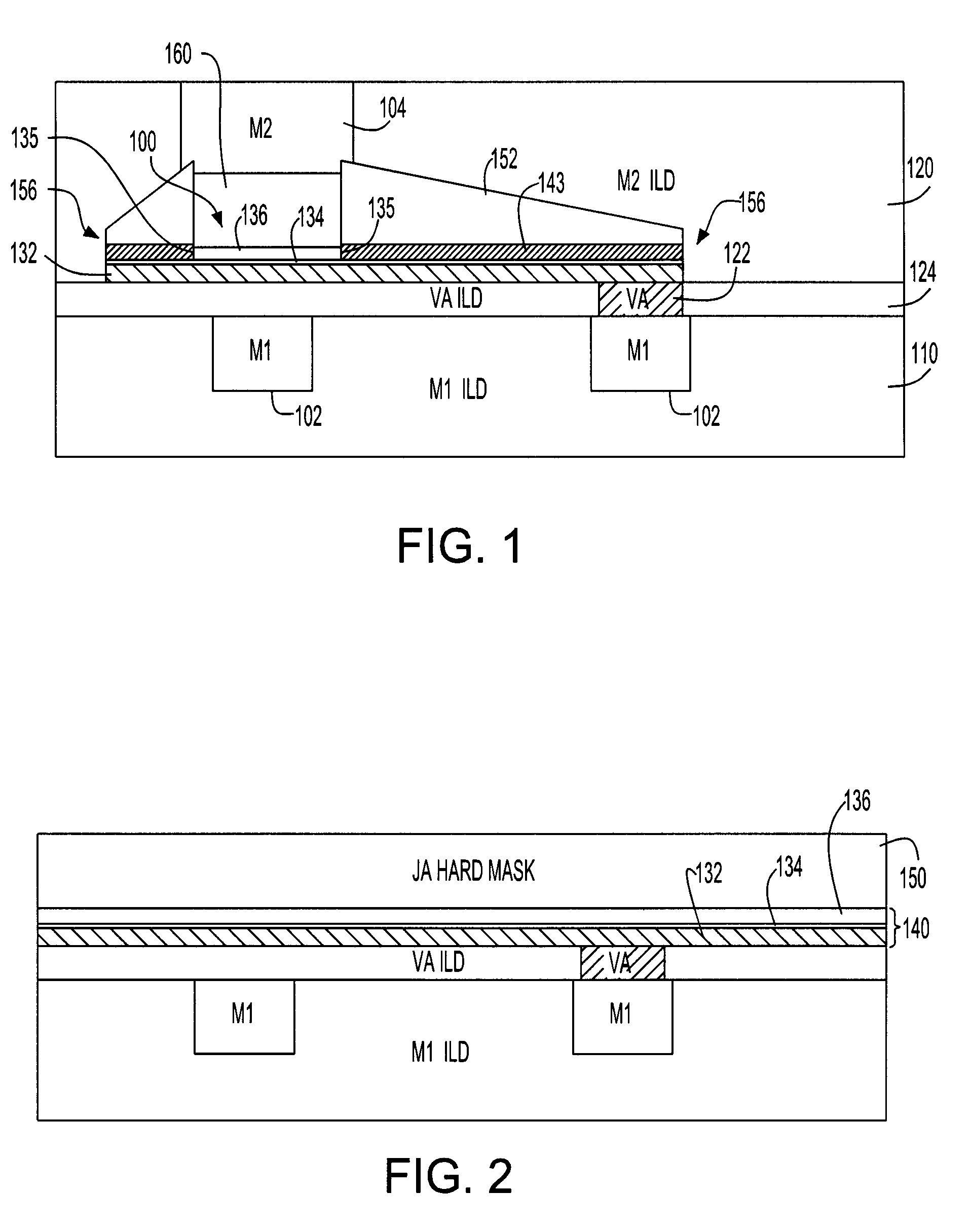
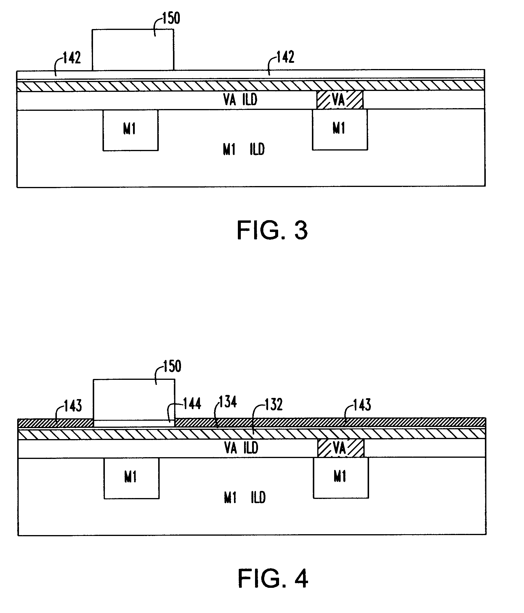
[0014]FIG. 1 is a cross-sectional view illustrating the structure of a patterned MTJ storage element 100 and its interconnection to M1 and M2 conductive lines. The MTJ 100 includes a pinned layer 132, a tunnel barrier layer 134 and a free layer 136. Each of these layers 132, 134, and 136 can include one or several layers which work together to enhance device performance or manufacturability. The free layer 136 is adjoined at first edges 135 of the MTJ by portions 143 of the free layer material that has been purposely inactivated. Preferably, the free layer 136 is also adjoined by the same type of inactivated material at second edges (not shown) in front of and in back of the MTJ 100, (the second edges not being visible in the particular cross-section shown), such that the MTJ 100 is surrounded by the same type of purposely inactivated material. The portions 143 of inactivated material extend to outer edges 156 of the patterned structure beyond the MTJ 100. The pinned layer 132 and t...


PUM


Abstract

A method of patterning a magnetic tunnel junction (MTJ) stack is provided. According to such method, an MTJ stack is formed having a free layer, a pinned layer and a tunnel barrier layer disposed between the free layer and the pinned layer. A first area of the MTJ stack is masked while the free layer of the MTJ is exposed in a second area. The free layer is then rendered electrically and magnetically inactive in the second area.

Description

BACKGROUND OF INVENTION [0001] The invention relates to microelectronic devices, and more particularly to a magnetic tunnel junction and method for patterning the same. [0002] In a magneto-resistive random access memory (MRAM), information is stored in arrays of magnetic storage elements known as magnetic tunnel junctions (MTJs). One of the advantages of MRAM is the capability of the MTJ storage array to be placed in a level above the surface of a semiconductor substrate. In that way, the surface area of the semiconductor substrate is conserved for use by relatively few transistors used to control the MTJ array. In addition, the available substrate surface area does not constrain the density of the MRAM to the same extent as in other types of memory. MRAM technology potentially offers great benefits to the integration of processors and other system elements on a single integrated circuit (IC or “chip”), commonly referred to as “systems on a chip” (SOCs). The placement of the MTJ arr...

Claims


Application Information

Patent Timeline
IPC IPC(8): G11C11/14G11C11/16H01L27/22H01L43/12
CPCG11C11/16H01L43/12H01L27/222H10N50/01
Inventor GAIDIS, MICHAEL C.ABRAHAM, DAVID W.BROWN, STEPHEN L.GUPTA, ARUNAVAPARK, CHANRORABERG, WOLFGANG
Owner INFINEON TECH AG
Features
  • Generate Ideas
  • Intellectual Property
  • Life Sciences
  • Materials
  • Tech Scout
  • Unparalleled Data Quality
  • Higher Quality Content
  • 60% Fewer Hallucinations
Learn More