Novel test structure for automatic dynamic negative-bias temperature instability testing

a technology of temperature instability and test structure, applied in the direction of logic circuits, pulse generation by logic circuits, electric pulse generators, etc., can solve the problems of complex nbti degradation mechanism, tedious phase making, and degeneration of device threshold characteristics, so as to minimize parasitic capacitance and lc coupling associated effects

Inactive Publication Date: 2005-12-15
CHARTERED SEMICONDUCTOR MANUFACTURING
View PDF7 Cites 32 Cited by
  • Summary
  • Abstract
  • Description
  • Claims
  • Application Information

AI Technical Summary

Benefits of technology

[0032] In addition, it is an objective of this invention to enable the testing to occur with exact test pulse train phas...

Problems solved by technology

The theory of the NBTI degradation mechanism is complex, but is generally believed to be caused by the generation of interface traps in the device silicon generated by negative bias and accelerated by high temperature.
These interface traps cause degeneration of device threshold characteristics, particularly for PMOS devices.
It is a tedious job...

Method used


Image

  • Novel test structure for automatic dynamic negative-bias temperature instability testing
  • Novel test structure for automatic dynamic negative-bias temperature instability testing
  • Novel test structure for automatic dynamic negative-bias temperature instability testing

Examples


Embodiment Construction

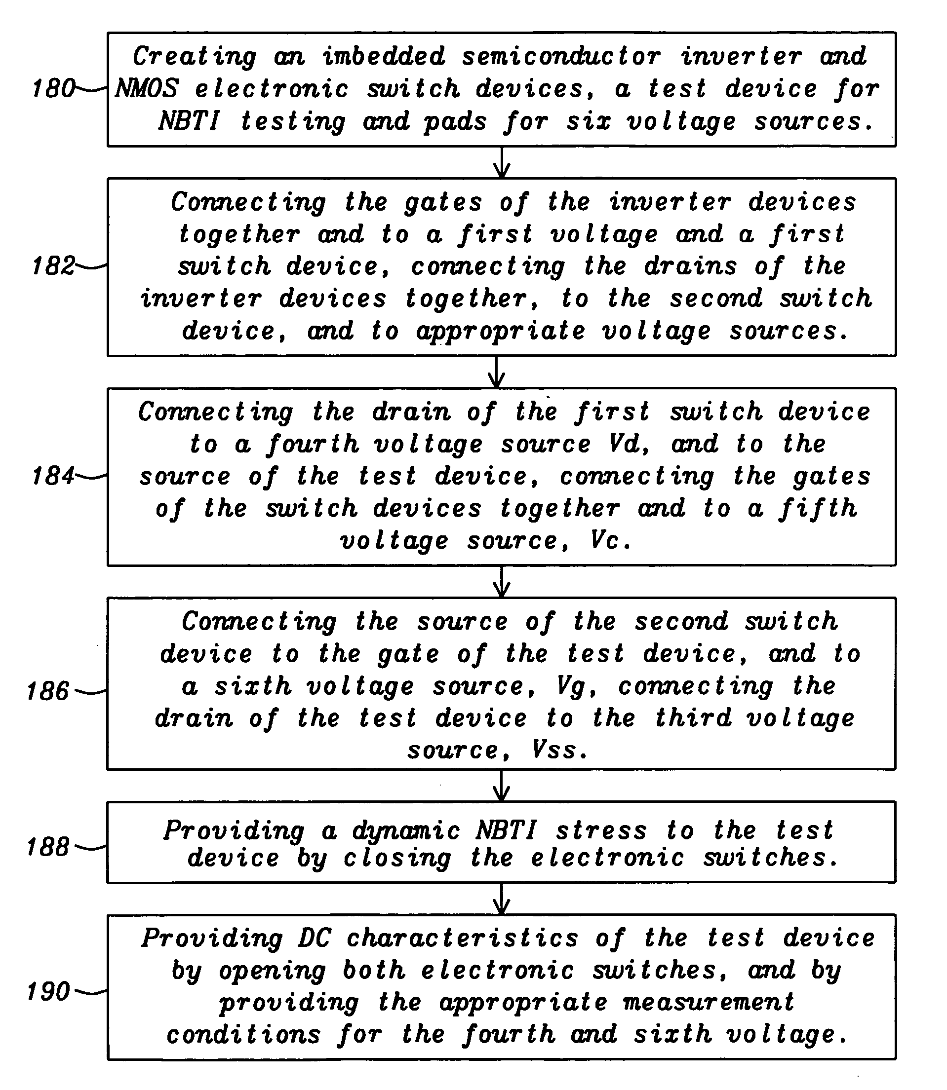
[0046]FIG. 4(A) shows one embodiment of the invention for simplified automatic dynamic testing of NBTI. The CMOS inverter 54 is incorporated into the silicon of the device to be tested.

[0047] The inverter consists of the PMOS device 56 in series with a NMOS device 58. The PMOS device 56 gate is connected to the gate of the NMOS device 58 and to a first voltage Vpulse input pad 52. The source of the PMOS device 56 is connected to a second voltage source Vdd. The gates are also connected to the source of the first integrated electronic switch 60. The drains of the two inverter FET devices are connected together and form the output of the inverter.

[0048] The inverter 54 output voltage Vout has a 180 degree phase relationship from the input first voltage Vpulse. This output Vout is then connected to the drain of the second integrated NMOS electronic switch 62.

[0049] The source of the inverter NMOS 58 is connected to a third voltage source, Vss, typically ground. The gates of the two ...


PUM


Abstract

The invention describes a novel test structure and process to create the structure for performing automatic dynamic stress testing of PMOS devices for Negative Bias Temperature Instability (NBTI). The invention consists of an integrated inverter, two integrated electronic switches for switching from stress mode to device DC characterization measurement mode, and a PMOS FET device under test (DUT). The inverter assures the proper 180 degree phase relationship between the test device source and gate voltage while the imbedded electronic switches provide isolation of the test device during DC characterization testing. Another embodiment of the invention enables the testing of multiple devices under test (DUT's).

Description

BACKGROUND OF THE INVENTION [0001] (1) Field of the Invention [0002] The present invention relates generally to a novel test structure and process for automatic Dynamic Negative-Bias Temperature Instability (DNBTI) testing of semiconductor devices to improve device reliability and performance. [0003] (2) Description of Prior Art [0004] As feature sizes for semiconductor devices decrease, along with the decrease in thickness of gate oxide layers, Negative Bias Temperature Instability (NBTI) has become an increasing reliability and performance concern. NBTI is not limited exclusively to short channel devices, but is directly related to device size reduction in the vertical direction. The theory of the NBTI degradation mechanism is complex, but is generally believed to be caused by the generation of interface traps in the device silicon generated by negative bias and accelerated by high temperature. These interface traps cause degeneration of device threshold characteristics, particula...

Claims


Application Information

Patent Timeline
IPC IPC(8): G01R31/26G06F17/50H01L23/544H01L25/00H03K19/00
CPCG01R31/2628G01R31/2642H01L22/34H01L2924/0002H01L2924/00
Inventor ANG, CHEW HOECHEN, GANGTAN, SHYUE SENG
Owner CHARTERED SEMICONDUCTOR MANUFACTURING
Why Eureka
Try Eureka