

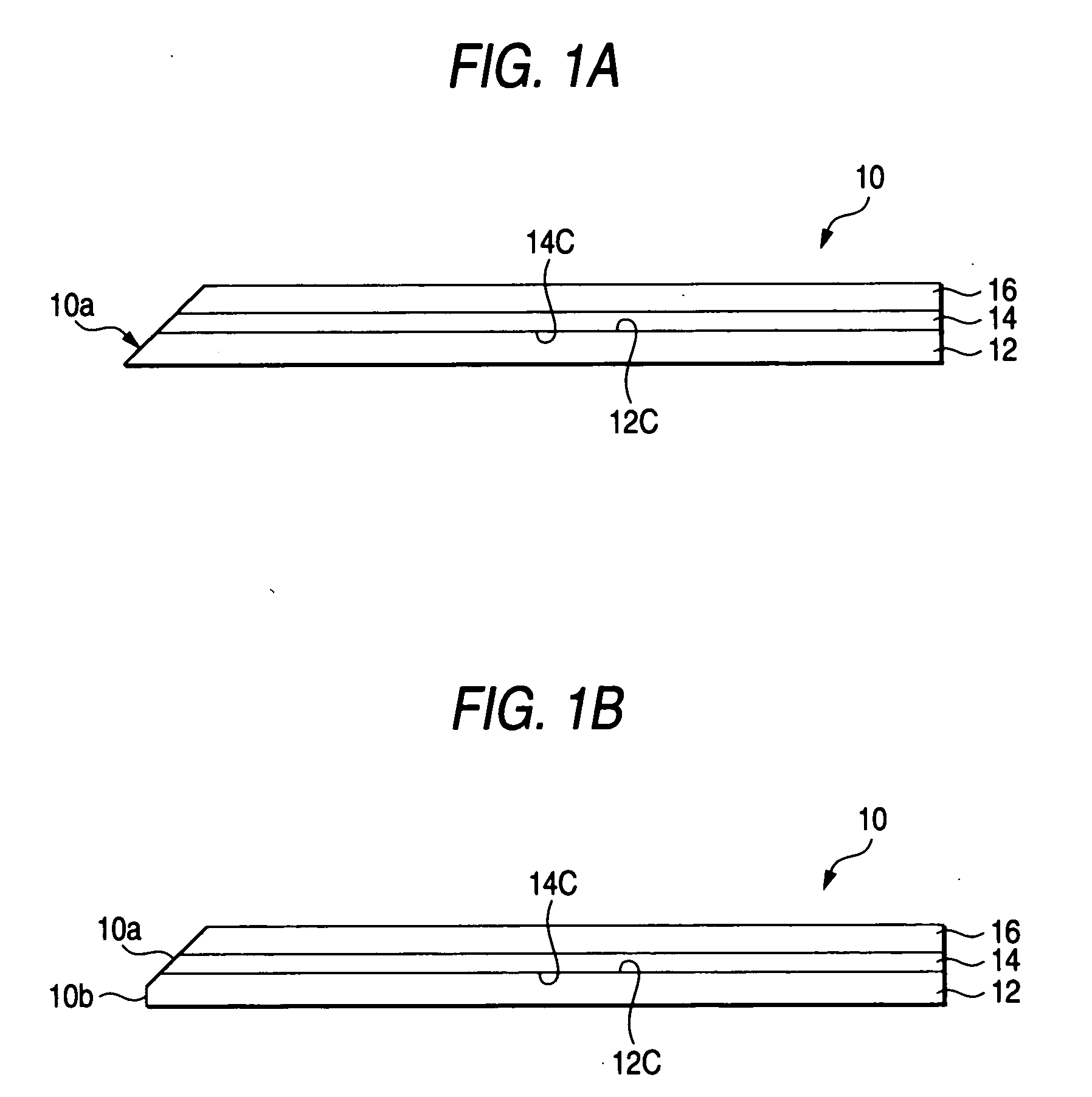
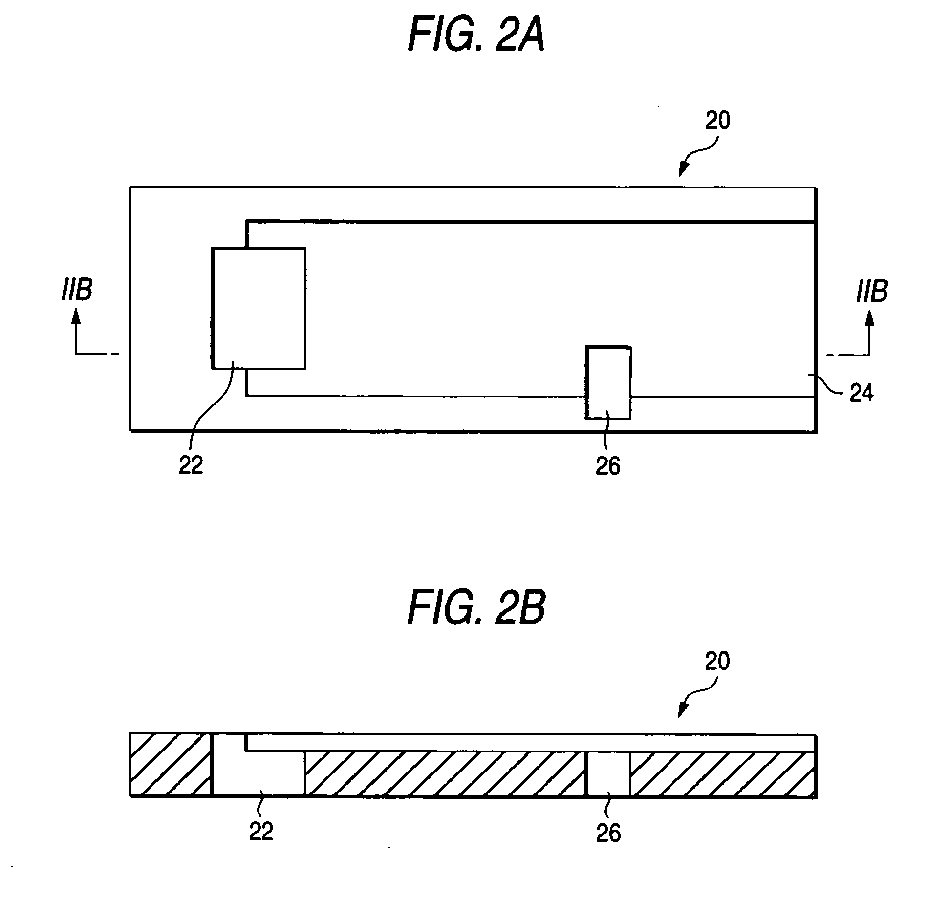
Polymeric optical waveguide film, polymeric optical waveguide module and method of manufacturing polymeric optical waveguide film
- Summary
- Abstract
- Description
- Claims
- Application Information
AI Technical Summary
Benefits of technology
Problems solved by technology
Method used
Image

Examples
example 1
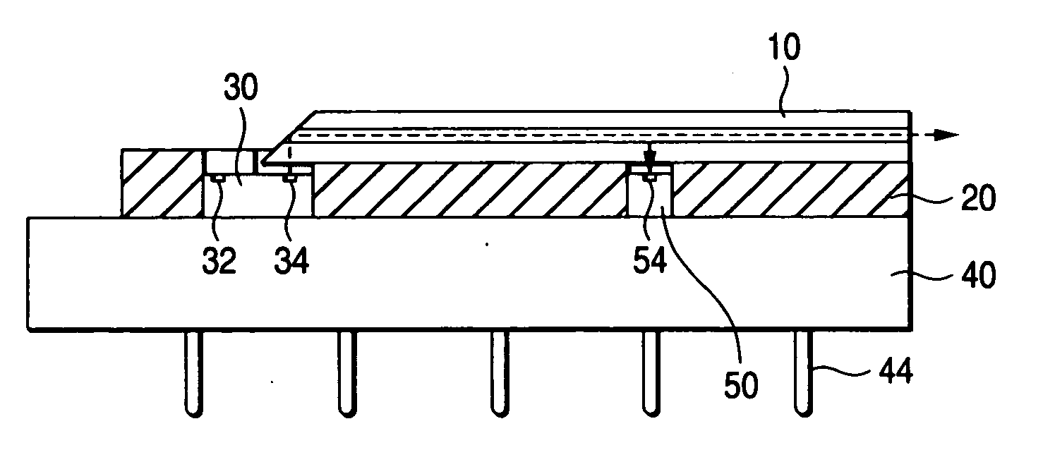
[0134] This Example is such that a polymeric optical waveguide module as shown in FIGS. 6 and 7A-7D is manufactured.
[0135] After a thick resist film (SU-8 of MicroChem Corp.) is applied to a Si substrate by spin coating, it is pre-baked at 80° C., exposed through a photomask, and developed, whereby four projections having a square cross section (50 μm in both width and height and 80 mm in length) are formed. The interval between the adjoining projections is set at 250 μm. The resulting substrate is post-baked at 120° C., whereby an original plate for manufacture of a polymeric optical waveguide is produced.
[0136] Then, after a mold release agent is applied to the original plate, a mixture of thermoplastic liquid dimethylsiloxane rubber (SYLGARD 184 of Dow Corning Asia Ltd.; viscosity: 5,000 mPa·s) and the curing agent is poured, cured by heating it at 120° C. for 30 minutes, and is peeled off, whereby a mold (thickness: 5 mm) having recesses corresponding to the projections having...
example 2
[0145] This Example is such that a polymeric optical waveguide module is manufactured in the same manner as in Example 1 except that guided light leakage portions are formed in the lower surfaces of the cores. After cores are formed on the clad film base material, 5-μm-deep cuts in the guided light leakage portions in the lower surfaces of the cores are formed only in the cores with a dicing saw perpendicularly to the longitudinal direction of the cores. The blade of the dicing saw has a grain size of about 7 μm and the surface is roughened by this blade.
example 3
[0146] A polymeric optical waveguide module with a light-emitting element is manufactured in the same manner as in Example 1 except that the light-emitting element is changed to a GaAs photodiode. Results are similar to the results of Example 1.
PUM
 Abstract
Description
Claims
Application Information