Method for fabricating semiconductor device

a semiconductor and device technology, applied in the direction of semiconductor devices, electrical devices, transistors, etc., can solve the problems of degrading the operating characteristic of the device, increasing the capacity of the bit line, slow operation speed of the device, etc., to prevent the increase of the parasitic capacity of the conductive pattern, the effect of preventing contact resistan

Active Publication Date: 2005-12-29
SK HYNIX INC
View PDF8 Cites 27 Cited by
  • Summary
  • Abstract
  • Description
  • Claims
  • Application Information

AI Technical Summary

Benefits of technology

[0013] It is, therefore, an object of the present invention to provide a method for fabricating a semiconductor device capable of preventing a contact resistance from increasing in a region contacted to an N-type conductive region during forming a conductive pattern directly contacted to the N-type conductive region including a conductive pattern and silicon, and preventing an increase in a parasitic capacity of the conductive pattern according to an increase in a thickness of a barrier layer.

Problems solved by technology

Accordingly, as for a high integrated device with a size of less than approximately 800 Å, a current capacity is decreased by an increase in a resistance of an N-channel metal-oxide semiconductor (NMOS) transistor and thus, an operating speed of the device becomes slow.
Therefore, a parasitic capacity of the bit line increases, thereby degrading an operating characteristic of the device.

Method used


Image

  • Method for fabricating semiconductor device
  • Method for fabricating semiconductor device
  • Method for fabricating semiconductor device

Examples


Embodiment Construction

[0021] Hereinafter, detailed descriptions on preferred embodiments of the present invention will be provided with reference to the accompanying drawings.

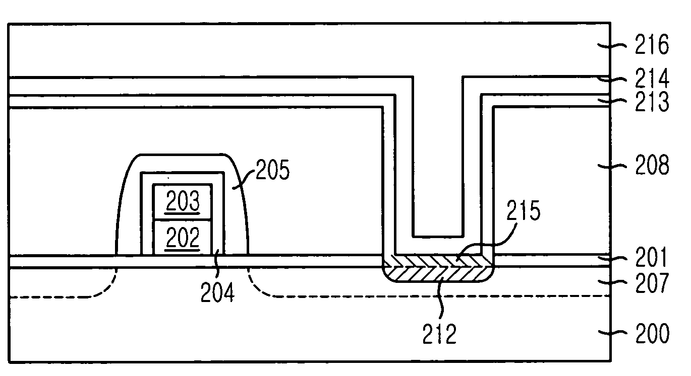
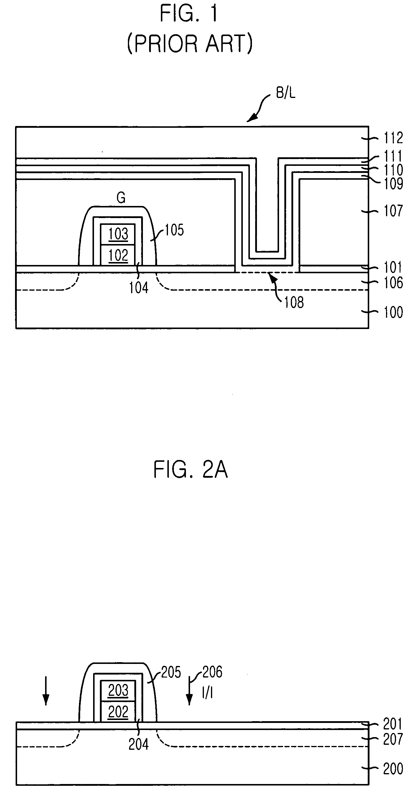
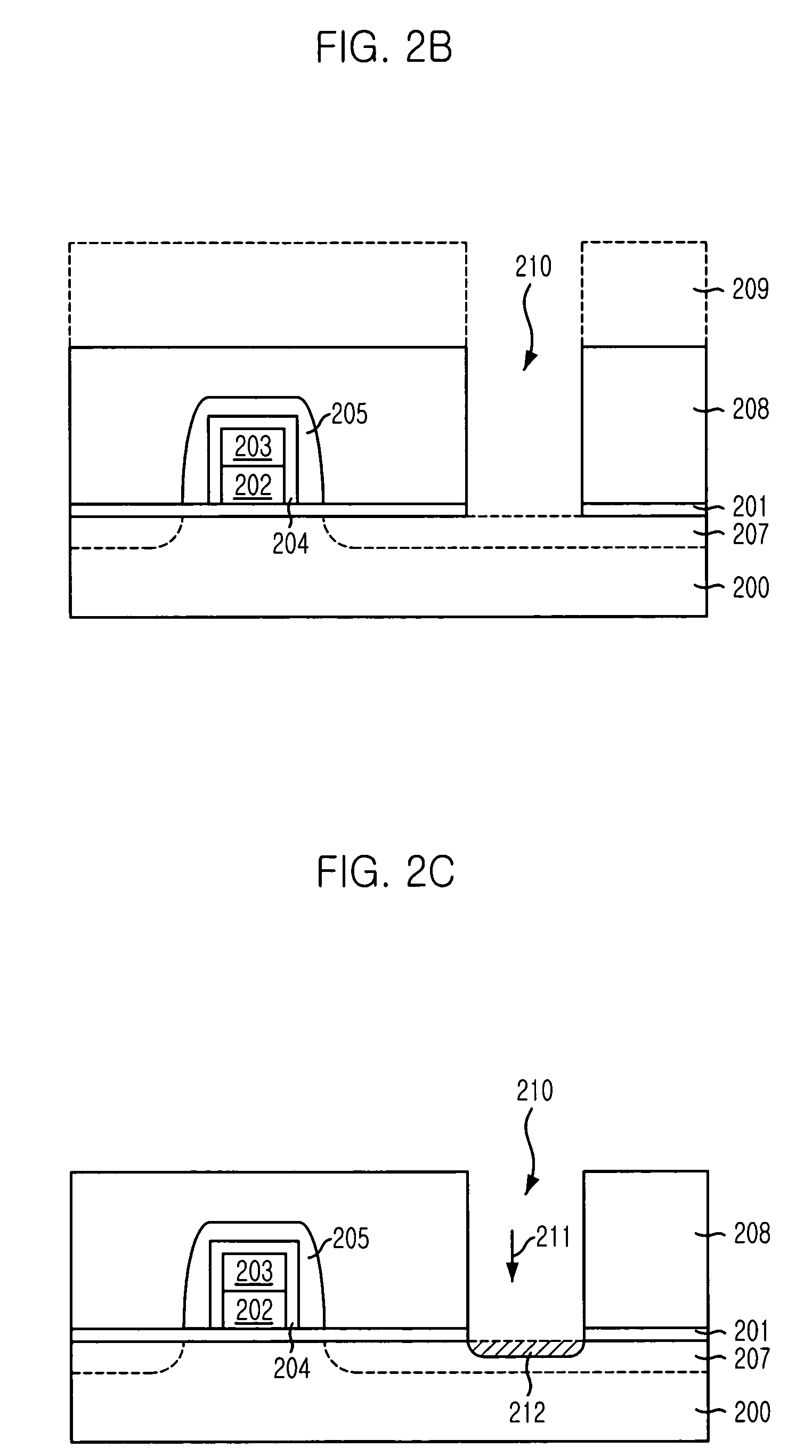
[0022]FIGS. 2A to 2E are cross-sectional views illustrating a process for forming a bit line in accordance with the present invention.

[0023] Hereinafter, with reference to FIGS. 2A to 2E, the present invention is explained as exemplifying the process for forming the bit line.

[0024] Referring to FIG. 2A, a gate insulation layer 201 is formed on a substrate 200 provided with various elements for forming a semiconductor device. The gate insulation layer 201 uses an oxide-based insulation layer. Herein, the substrate 200 is a typical silicon substrate.

[0025] A conductive layer and an insulation layer for a hard mask are sequentially deposited on the gate insulation layer 201 and then, a mask pattern for a gate electrode pattern formation is formed through a photolithography process. Thereafter, the conductive layer and the insulatio...


PUM


Abstract

The present invention provides a method for fabricating a semiconductor device capable of preventing a contact resistance from increasing in a region contacted to an N-type conductive region during forming a conductive pattern directly contacted to the N-type conductive region including a conductive pattern and silicon, and preventing an increase in a parasitic capacity of the conductive pattern according to an increase in a thickness of a barrier layer.

Description

FIELD OF THE INVENTION [0001] The present invention relates to a method for fabricating a semiconductor device; and more particularly, to a method for fabricating a semiconductor device capable of decreasing a contact resistance between a conductive region including silicon and a conductive pattern. DESCRIPTION OF RELATED ARTS [0002] A dynamic random access memory (DRAM) of a semiconductor memory device is divided into two regions. One is a cell region including a plurality of unit cells consisted of a transistor and a capacitor (1T1C) and the other is a peripheral region. [0003] For instance, a bit line is a line practically transmitting data and is connected to a source of a cell transistor. As for the cell region, the bit line is electrically interconnected to a cell contact plug contacted to a source / drain junction region of a gate electrode through a bit line contact plug. As for the peripheral region including a bit line sense amplifier for sensing and amplifying the cell data...

Claims


Application Information

Patent Timeline
Patent Type & Authority Applications(United States)
IPC IPC(8): H01L21/285H01L21/425H01L21/44H01L21/4763H01L27/108H01L21/768H01L21/8238H01L21/8242H01L29/49
CPCH01L21/28512H01L21/28518H01L21/76843H01L21/76846H01L29/4975H01L21/76877H01L27/10885H01L27/10888H01L21/76864H10B12/485H10B12/482H01L21/768H10B12/00
Inventor LEE, JOO-WANKIM, JUN-KI
Owner SK HYNIX INC
Why Eureka
Try Eureka