Supercharge Your Innovation With Domain-Expert AI Agents!

Display device, method of production of the same, and projection type display device

a display device and display method technology, applied in non-linear optics, instruments, optics, etc., can solve the problems of insufficient security of the light shielding area, the image quality is already affected, and the request for higher luminance is contrary to the request for higher luminance, so as to achieve the effect of high numerical aperture of pixels, high light resistance of pixel transistors, and reduced production costs

Inactive Publication Date: 2006-01-05
SONY CORP
View PDF4 Cites 0 Cited by
  • Summary
  • Abstract
  • Description
  • Claims
  • Application Information

AI Technical Summary

Benefits of technology

The present invention provides a display device with high light resistance of the pixel transistors without relying on a light shielding structure. This is achieved by integrating a display unit and a peripheral drive unit on a substrate, with both the pixel transistors and peripheral transistors being made of thin film transistors obtained by stacking polycrystalline semiconductor thin films and gate electrodes via gate insulating films. The average crystal grain size of the semiconductor thin film of the pixel transistors is smaller than the average crystal grain size of the semiconductor thin film of the peripheral transistors, resulting in a higher light resistance of the pixel transistors. The method of production involves forming a polycrystalline silicon film or a polycrystalline silicon film with a thinner active layer of the pixel transistors. The recrystallization step controls the average crystal grain size of the polycrystalline silicon film to 300 nm or less for the pixel transistors and 800 nm or more for the peripheral transistors. The invention provides a display device with high light resistance and a method of production that ensures high production efficiency.

Problems solved by technology

An increase of the photo-leakage current becomes a cause of flicker and roughness of the screen, so gives a fatal defect to the image quality.
However, the light shielding structure inevitably sacrifices the numerical aperture of the pixels, so runs contrary to the requests for higher luminance of the screen.
Due to the necessity of improvement of the numerical aperture of the liquid crystal display panel, it has already become difficult to sufficiently secure the light shielding area.

Method used


Image

  • Display device, method of production of the same, and projection type display device
  • Display device, method of production of the same, and projection type display device
  • Display device, method of production of the same, and projection type display device

Examples


Embodiment Construction

[0039] Below, a detailed explanation will be given of embodiments of the present invention in relation to the drawings.

[0040]FIG. 3 is a schematic view of an embodiment of a display device according to the present invention, in which FIG. 3A shows a layout of a display unit and a drive unit formed at a display panel; and FIG. 3B shows a sectional structure of the display panel cut along for example a line B-B of FIG. 3A.

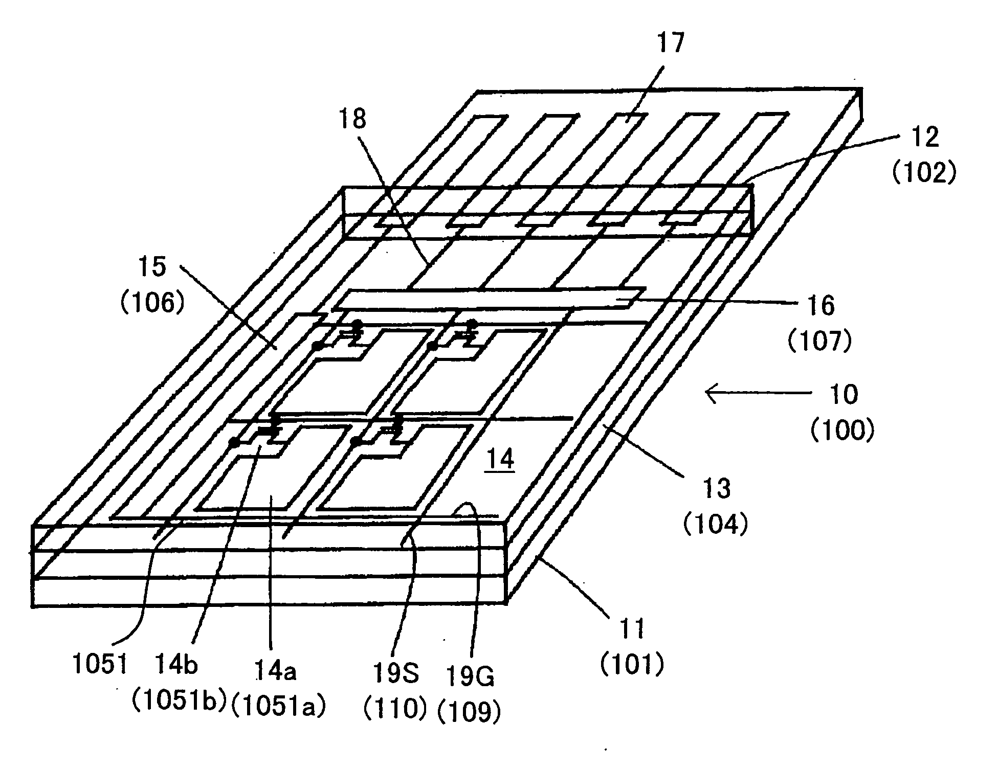
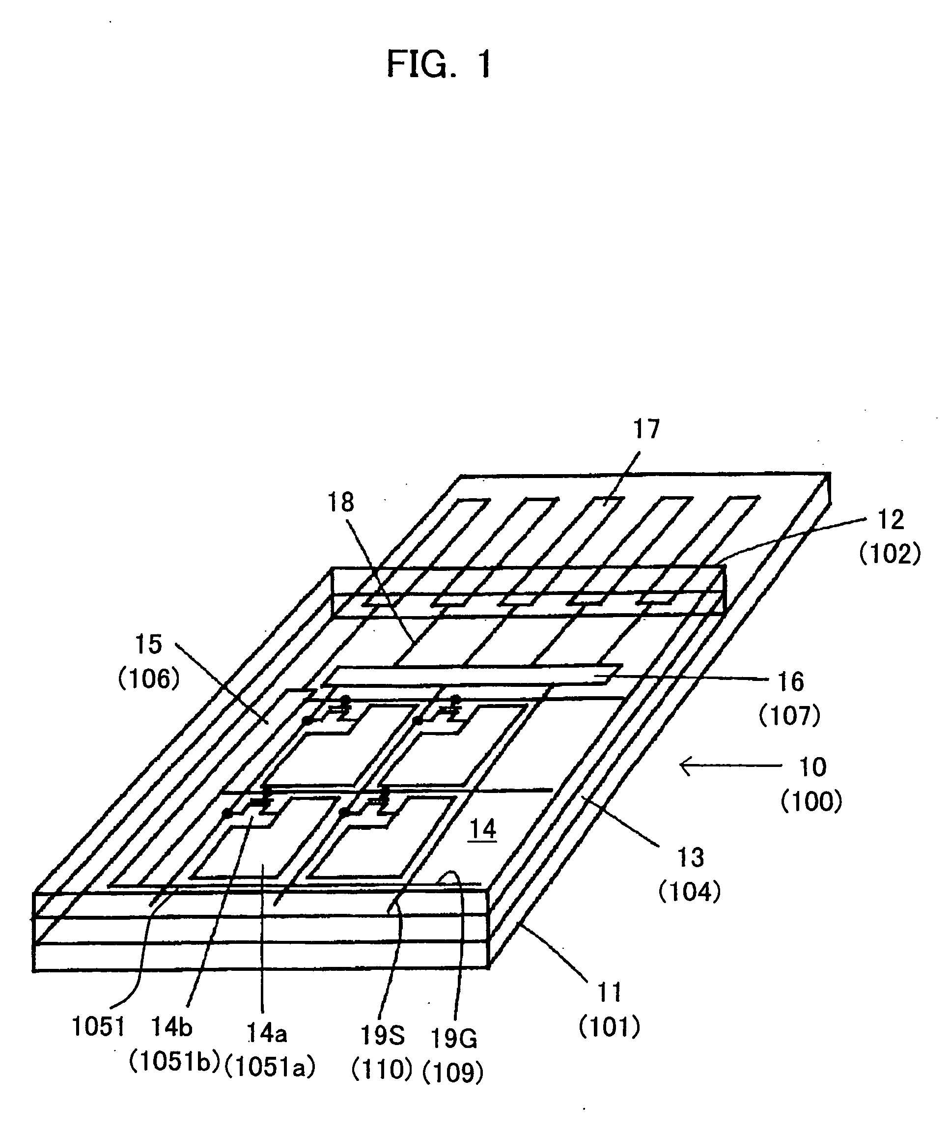
[0041] A display panel 100 has, as shown in the figure, a flat structure obtained by bonding a pair of glass substrates 101 and 102 by a sealing material 3. A gap between the pair of glass substrates 101 and 102 is filled with for example a liquid crystal 104 as an electrooptic material. In some cases, use can be made of another electrooptic material in place of a liquid crystal. The surface of the glass substrate 101, as shown in FIG. 3A, is integrally formed with the display unit and the peripheral drive unit. The inner surface of the glass substrate 102 facing t...


PUM

PropertyMeasurementUnit
average crystal grain sizeaaaaaaaaaa
thicknessaaaaaaaaaa

Abstract

A display device able to raise a light resistance of pixel transistors without depending upon a light shielding structure and a method of production of same, wherein an average crystal grain size of a polycrystalline silicon film 111 forming an active layer of the pixel transistors is controlled to be relatively small so as to suppress a photo-leakage current. The smaller the crystal grain size, the larger the included crystal defects. Carriers excited by light irradiation are smoothly captured by a defect level, and an increase of a photo-leakage current is suppressed. On the other hand, the average crystal grain size of the polycrystalline silicon film 111 constituting the peripheral transistors is controlled so as to become relatively large. The larger the crystal grain size, the larger the mobility of the carriers, and the higher the drivability of the peripheral transistors. This is because a higher speed operation is required for the peripheral transistors than the pixel transistors due to scanning of pixels and sampling of image signals.

Description

TECHNICAL FIELD [0001] The present invention relates to a flat type display device represented by a liquid crystal display device (LCD), a method of production of the same, and a projection type display device. In more detail, the present invention relates to an active matrix type display comprised of an active matrix configuration pixel array (display unit) and a peripheral drive unit integrally formed, a method of production of the same, and a projection type display device. Further concretely, it relates to the configuration of a thin film transistor included in the display unit and the drive unit. BACKGROUND ART [0002]FIG. 1 is a schematic perspective view showing an overall configuration of a general active matrix type display device. [0003] As shown in FIG. 1, this display device has a flat structure comprising a display panel 10 and provided with a pair of glass substrates 11 and 12 and an electrooptic material held between them. As the electrooptic material, use is made of f...

Claims


Application Information

Patent Timeline
Patent Type & Authority Applications(United States)
IPC IPC(8): H01L29/04G02F1/1362G02F1/1368H01L21/20H01L21/336H01L21/77H01L21/84H01L27/12H01L29/786
CPCG02F1/13454G02F1/1368G02F2202/104H01L21/2022H01L21/2026H01L27/1285H01L29/04H01L29/66757H01L29/78609H01L29/78633H01L29/78675H01L27/12H01L21/02532H01L21/0262H01L21/02675G02F1/136
Inventor MAKIMURA, SHINGOHASHIMOTO, MAKOTOOKAWA, YOSHIROWADA, TOMOHIROKATAOKA
Owner SONY CORP
Features
  • R&D
  • Intellectual Property
  • Life Sciences
  • Materials
  • Tech Scout
  • Unparalleled Data Quality
  • Higher Quality Content
  • 60% Fewer Hallucinations
Learn More